ZC0301 Просмотр технического описания (PDF) - Unspecified
Номер в каталоге
Компоненты Описание
Список матч
ZC0301 Datasheet PDF : 15 Pages
| |||
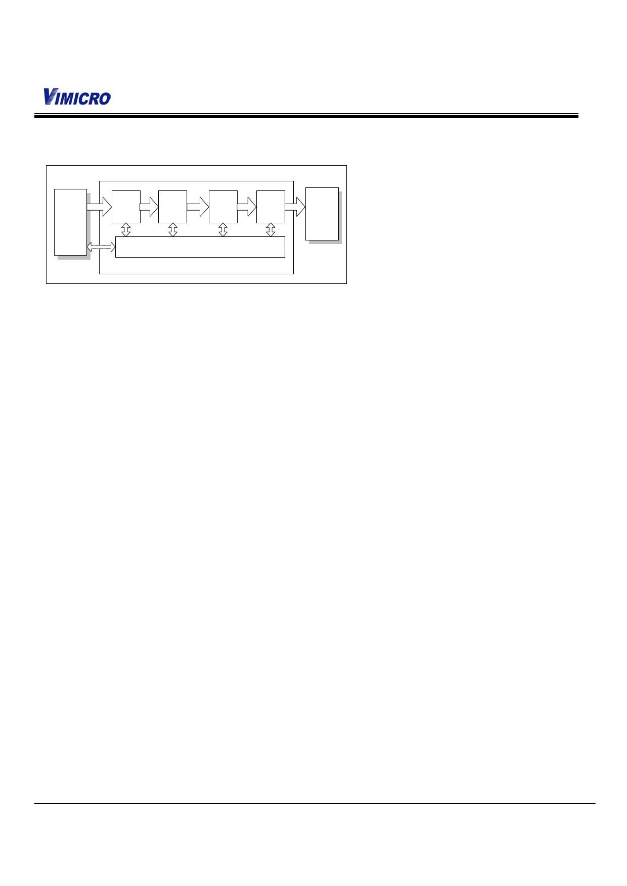
2. Architecture
ZC0301
VGA & CIF USB PC Camera Controller
CMOS
image
sensor
ISP
Sub-
sample &
Raster
JPEG
Encoder
USB
Device
Controller
PC
host
System Controller
ZC0301
Figure 2 ZC0301 Functional Block Diagram
The ZC0301 consists of five major function blocks, System Controller, Image Signal Processor, Sub-Sample & Raster,
JPEG Encoder, and USB Device Controller, as illustrated in Figure 1. These blocks provide the following functions.
2.1. System Controller
• Providing the control to ISP, JPEG, and USB blocks
• Configuring the control registers
• Chip clock generation
• Error control for the data block through USB interface
2.2. Image Signal Processor
• Dedicated sensor control and signal processing module.
• Serial-Bus interface for CMOS Image Sensor
• 8 bit Bayer format image input
• 3x3 Interpolation
• Color Correction
• Gamma Correction
• Automatic Exposure Control
• Automatic White Balance Control
• Programmable AE windows
• Automatic Reset Level Control
• RGB to YCrCb Color Space Convert
• Histogram Equalization Logic
2.3. Sub-Sample & Raster
• The input data format is 4:4:4 for Y component, Cb component and Cr component. The three components for a
pixel are input simultaneously.
5
Mar. 2002
Share Link: 