V62C2184096LL-70B Просмотр технического описания (PDF) - Mosel Vitelic, Corp
Номер в каталоге
Компоненты Описание
Список матч
V62C2184096LL-70B Datasheet PDF : 10 Pages
| |||
MOSEL VITELIC
V62C2184096
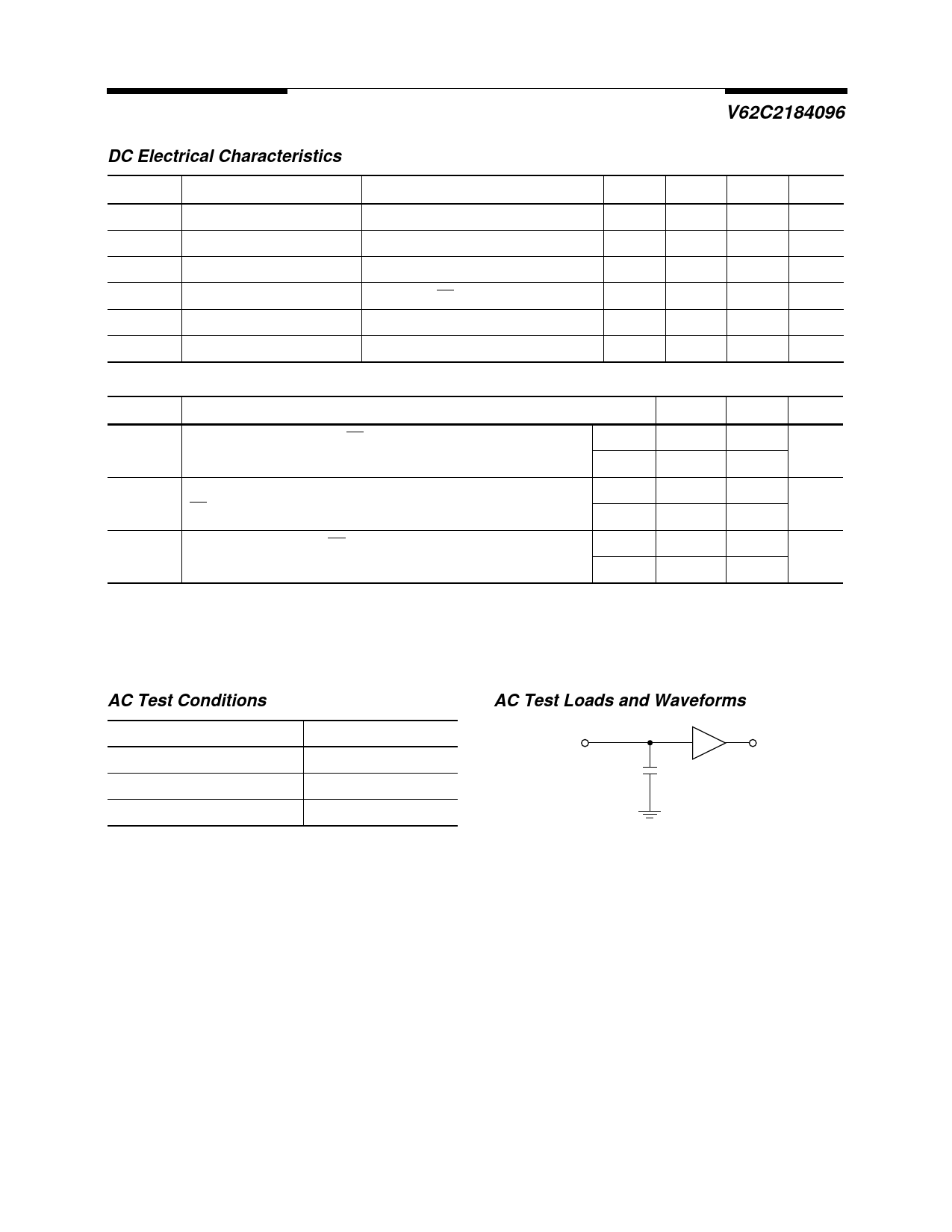
DC Electrical Characteristics (over all temperature ranges, VCC = 2.3V–3.0V)
Symbol
VIL
VIH
IIL
IOL
VOL
VOH
Parameter
Input LOW Voltage(1,2)
Input HIGH Voltage(1)
Input Leakage Current
Output Leakage Current
Output LOW Voltage
Output HIGH Voltage
Test Conditions
Min.
-0.5
2.0
VCC = Max, VIN = 0V to VCC
—
VCC = Max, CE1 = VIH, VOUT = 0V to VCC
—
VCC = Min, IOL = 2mA
—
VCC = Min, IOH = -0.5mA
VCC–0.4
Typ.
—
—
—
—
—
—
Max. Units
0.4
V
VCC+0.3
V
1
µA
1
µA
0.4
V
—
V
Symbol Parameter
Comm.(3) Ind.(3) Units
ICC1
Average Operating Current, CE1 = VIL, CE2 = VCC – 0.2, Output Open, f = fmax
35
VCC = Max.
f = 1 MHz
4
40
mA
5
ISB
TTL Standby Current
CE1 ≥ VIH, CE2 ≤ VIL, VCC = Max., f = 0
L
0.5
1
mA
LL
0.3
1
ISB1
CMOS Standby Current, CE1 ≥ VCC – 0.2V, CE2 ≤ 0.2V,
VIN ≥ VCC – 0.2V or VIN ≤ 0.2V, VCC = Max., f = 0
L
10
15
µA
LL
5
7
NOTES:
1. These are absolute values with respect to device ground and all overshoots due to system or tester noise are included.
2. VIL (Min.) = -3.0V for pulse width < tRC/2.
3. Maximum value.
AC Test Conditions
Input Pulse Levels
Input Rise and Fall Times
Timing Reference Levels
Output Load
0 to 2.0V
5 ns
1.1V
see below
AC Test Loads and Waveforms
CL* TTL
CL = 30pF + 1TTL Load
* Includes scope and jig capacitance
V62C2184096 Rev. 1.5 June 2000
4
Share Link: 