V62C2164096L-70T Просмотр технического описания (PDF) - Mosel Vitelic, Corp
Номер в каталоге
Компоненты Описание
Список матч
V62C2164096L-70T Datasheet PDF : 10 Pages
| |||
MOSEL VITELIC
V62C2164096
Pin Descriptions
A0–A17
Address Inputs
These 18 address inputs select one of the 256K x
16 bit segments in the RAM.
CE1, CE2* Chip Enable Inputs
CE1 is active LOW and CE2 is active HIGH. Both
chip enables must be active to read from or write to
the device. If either chip enable is not active, the
device is deselected and is in a standby power
mode. The I/O pins will be in the high-impedance
state when deselected.
OE
Output Enable Input
The output enable input is active LOW. With chip
enabled, when OE is Low and WE High, data will
be presented on the I/O pins. The I/O pins will be in
the high impedance state when OE is High.
UBE, LBE Byte Enable
Active low inputs. These inputs are used to enable
the upper or lower data byte.
WE
Write Enable Input
The write enable input is active LOW and controls
read and write operations. With the chip enabled,
when WE is HIGH and OE is LOW, output data will
be present at the I/O pins; when WE is LOW and
OE is HIGH, the data present on the I/O pins will be
written into the selected memory locations.
I/O1–I/O16 Data Input and Data Output Ports
These 16 bidirectional ports are used to read data
from and write data into the RAM.
VCC
GND
Power Supply
Ground
*CE2 is available on BGA package only.
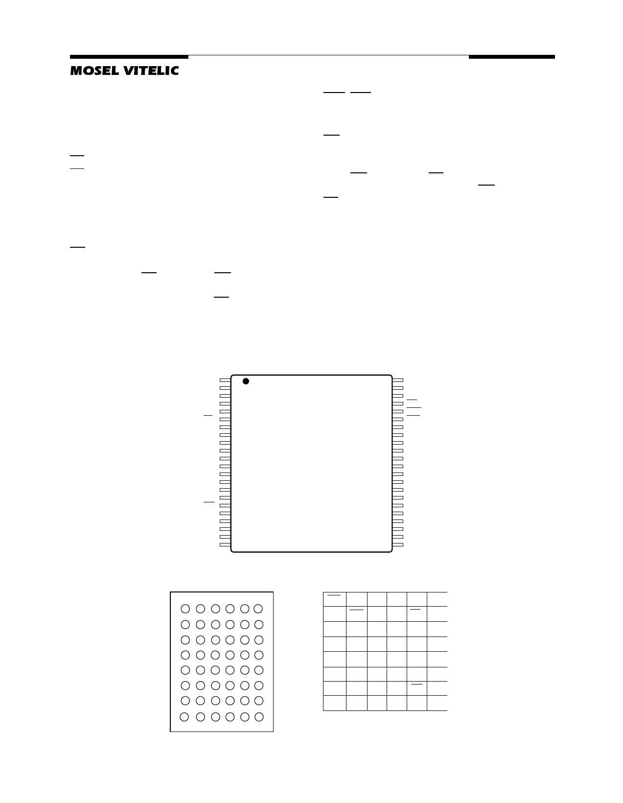
Pin Configurations (Top View)
44-Pin TSOP-II (Standard)
A4
1
A3
2
A2
3
A1
4
A0
5
CE1
6
I/O1
7
I/O2
8
I/O3
9
I/O4
10
VCC
11
GND
12
I/O5
13
I/O6
14
I/O7
15
I/O8
16
WE
17
A15
18
A14
19
A13
20
A12
21
A16
22
44
A5
43
A6
42
A7
41
OE
40
UBE
39
LBE
38
I/O16
37
I/O15
36
I/O14
35
I/O13
34
GND
33
VCC
32
I/O12
31
I/O11
30
I/O10
29
I/O9
28
NC
27
A8
26
A9
25
A10
24
A11
23
A17
1 23456
A
B
C
D
E
F
G
H
TOP VIEW
48 BGA
123
A BLE OE A0
B I/O9 BHE A3
C I/O10 I/O11 A5
4 56
A1 A2 CE2
A4 CE1 I/O1
A6 I/O2 I/O3
D VSS I/O12 A17 A7 I/O4 VCC
E VCC I/O13 NC A16 I/O5 VSS
F I/O15 I/O14 A14 A15 I/O6 I/O7
G I/O16 NC A12 A13 WE I/O8
H NC A8 A9 A10 A11 NC
Note: NC means no connect.
TOP VIEW
V62C2164096 Rev. 1.0 November 2001
2
Share Link: 