U3500BM Просмотр технического описания (PDF) - Temic Semiconductors
Номер в каталоге
Компоненты Описание
Список матч
U3500BM Datasheet PDF : 17 Pages
| |||
U3500BM
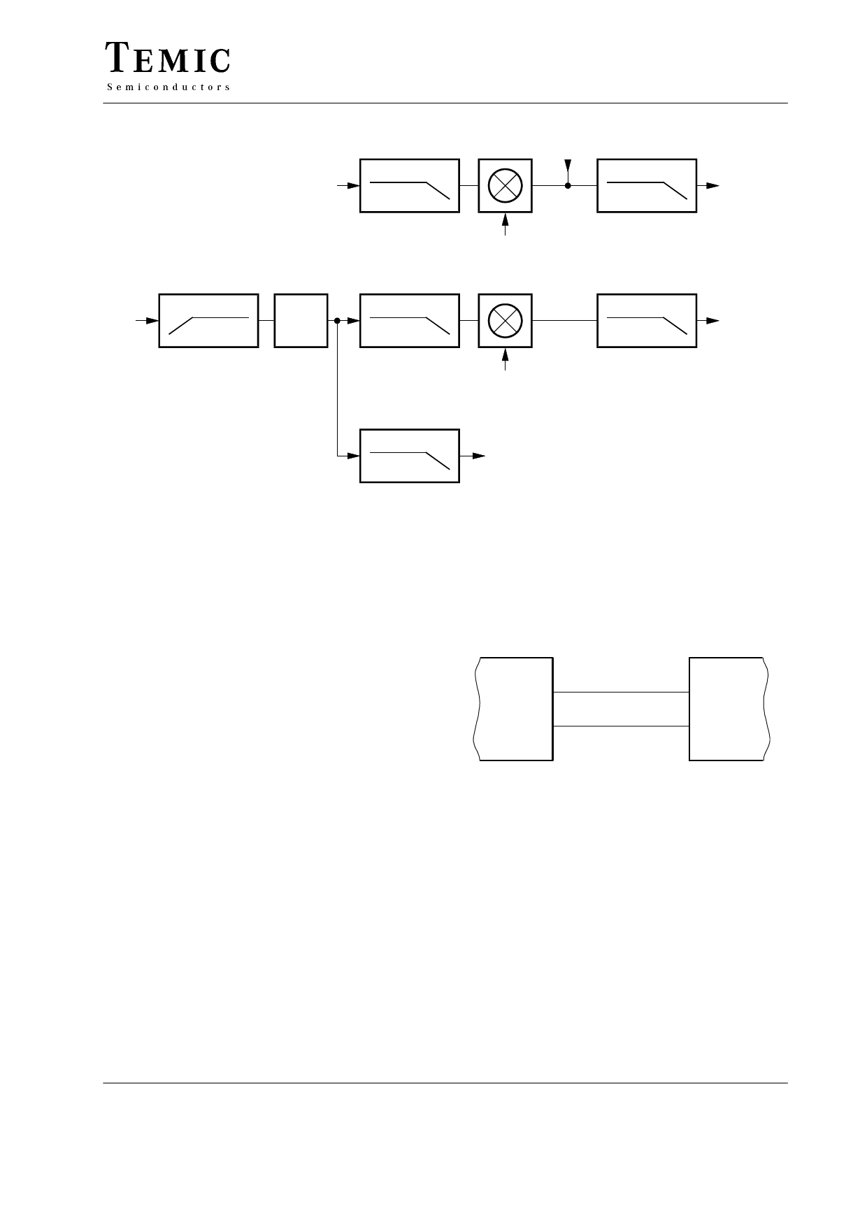
Gain stage
F–3 dB=3.35 kHz
DATA
F–3 dB=3.95 kHz
Output buffer
Demo–
dulator
F–3 dB=90 Hz
RGAIN
ADJ
Signal: 4.1 kHz/DC/OFF
State : SCRON/SCROFF/DATA
Gain : –4 dB/0 dB/OFF
F–3 dB=3.95 kHz
Signal: 1 kHz
State : SCRON/SCROFF
Gain : 5.9 dB/1.9 dB
F–3 dB=3.35 kHz
Deemphasis
DATA
Signal: 4.1 kHz/DC/OFF
State : DESCRON/DESCROFF/DATA
Gain : –4 dB/0 dB/OFF
F–3 dB=1 kHz
Comparator
Figure 11.
Signal: 1 kHz
State : DESCRON/DESCROFF
Gain : –0.5 dB/–4.5 dB
11786
Serial Bus Interface
The circuit is remoted by an external microcontroller
through the serial bus (programming can be started 10 ms
after power supply settled).
The data is an 12-bit word:
A3 – A0: address of the destination register (0 to 15)
D7 – D0: contents of register
The data line must be stable when the clock is high and
data must be serially shifted.
After 12 clock periods, the transfer to the destination reg-
ister is (internally) generated by a low-to-high transition
of the data line when the clock is high.
Micro-
processor
Data
Clock
Figure 12.
D
C
96 11787
Rev. A3, 20-May-98
Preliminary Information
11 (17)
Share Link: 