CS5126 Просмотр технического описания (PDF) - Cirrus Logic
Номер в каталоге
Компоненты Описание
Список матч
CS5126 Datasheet PDF : 32 Pages
| |||
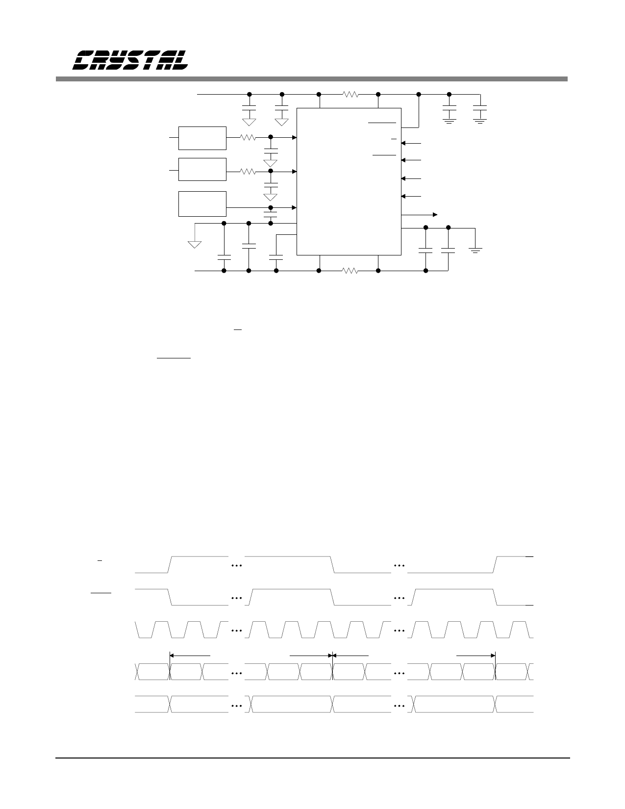
CS5126
Left Ch.
Analog In
Right Ch.
Analog In
+5V
+ 1 µF 0.1µF
10Ω
0.1µF
+ 1 µF
VA+
VD+
Anti Alias
Filter
Anti Alias
Filter
Voltage
Reference
200Ω
1 nF
200Ω
1 nF
1 µF +
0.1µF
AINL
SLEEP
L/R
fclk /512
HOLD
AINR CS5126
SCLK
fclk /256
fclk /16
VREF
AGND
REFBUF
VA-
CLKIN
f clk
SDATA
DGND
0.1µF
VD-
+ 1 µF
0.1µF
10Ω
-5V
Figure 2. Stereo Mode Connection Diagram
each conversion finishes determines which chan-
nel is acquired and tracked. The L/R input must
remain valid at least until 30ns before the next
falling transition on HOLD.
As shown in the timing diagram in Figure 3, the
CS5126 uses pipelined data transmission. That
is, data from a particular conversion transmits
during the next conversion cycle. The serial
clock input, SCLK, is derived by dividing the
master clock by 16. The MSB (most-significant-
bit) will be stable on the first rising edge of
SCLK after a falling transition on HOLD. With
a serial clock of fclk/16, transmission of all 16
output bits will span an entire conversion and
acquisition cycle.
STEREO MODE PERFORMANCE
As illustrated in Figure 4, the CS5126 typically
provides 92dB S/(N+D) and 0.001% THD. Un-
like conventional successive-approximation
ADC’s, the CS5126’s signal-to-noise and dy-
namic range are not limited by differential non-
linearities (DNL) caused by calibration errors.
Rather, the dominant noise source is broadband
thermal noise which aliases into the baseband.
This white broadband noise also appears as an
idle channel noise of 1/2 LSB (rms).
L/R (i)
HOLD (i)
SCLK (i)
SDATA (o) LSB MSB
Left Channel Data
LSB MSB
Right Channel Data
LSB MSB
Internal
Status
Rch Conv.
Lch Acq.
Lch Conv.
Figure 3. Stereo Mode Timing
Rch Acq.
DS32F1
7
Share Link: 