MC74HC367AN Просмотр технического описания (PDF) - ON Semiconductor
Номер в каталоге
Компоненты Описание
Список матч
MC74HC367AN Datasheet PDF : 6 Pages
| |||
MC74HC367A
Hex 3−State Noninverting
Buffer with Separate 2−Bit
and 4−Bit Sections
High−Performance Silicon−Gate CMOS
The MC74HC367A is identical in pinout to the LS367. The device
inputs are compatible with standard CMOS outputs; with pullup
resistors, they are compatible with LSTTL outputs.
This device is arranged into 2−bit and 4−bit sections, each having its
own active−low Output Enable. When either of the enables is high, the
affected buffer outputs are placed into high−impedance states. The
HC367A has noninverting outputs.
• Output Drive Capability: 15 LSTTL Loads
• Outputs Directly Interface to CMOS, NMOS, and TTL
• Operating Voltage Range: 2 to 6 V
• Low Input Current: 1 μA
• High Noise Immunity Characteristic of CMOS Devices
• In Compliance with the Requirements Defined by JEDEC Standard
No. 7A
• Chip Complexity: 92 FETs or 23 Equivalent Gates
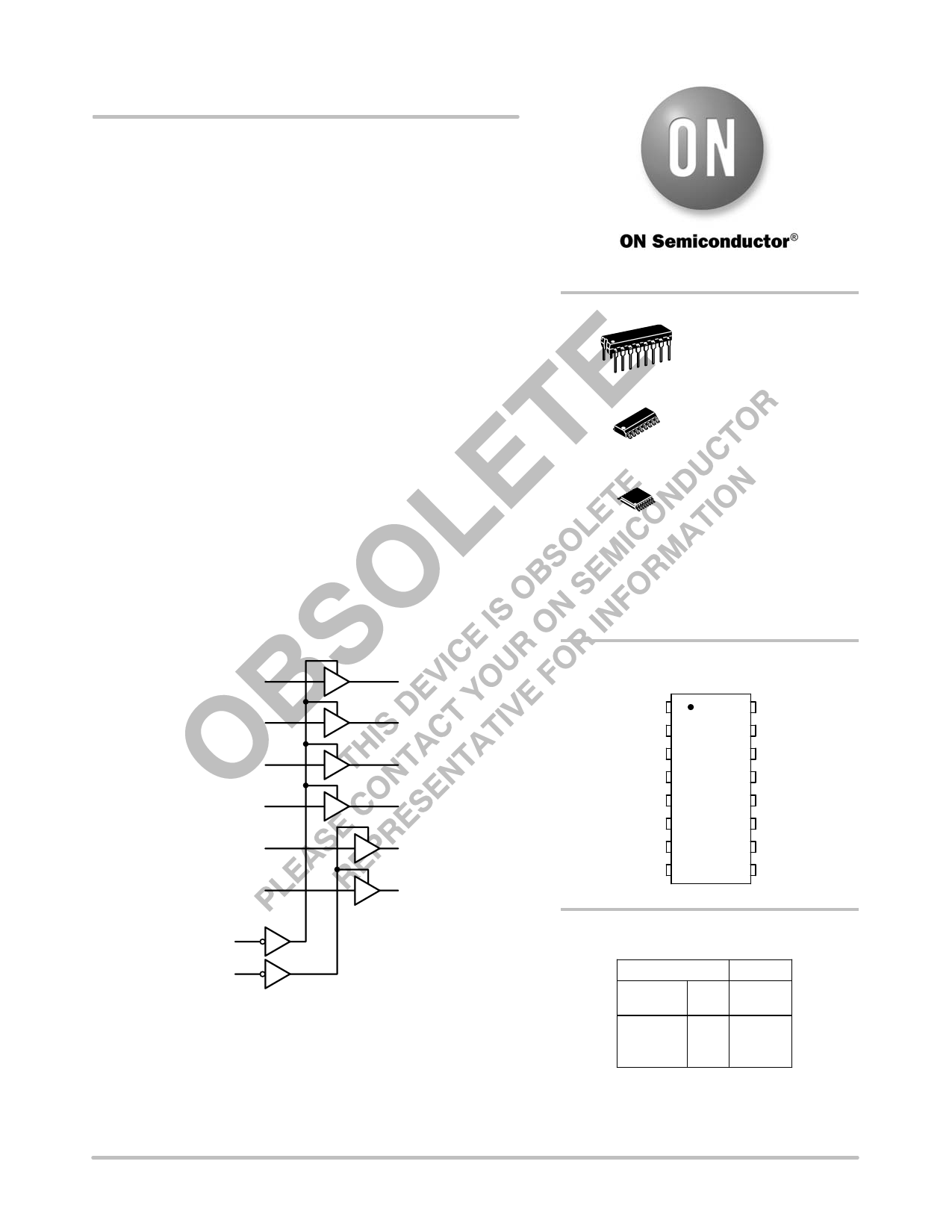
LOGIC DIAGRAM
A0 2
A1 4
A2 6
A3 10
A4 12
A5 14
3 Y0
5 Y1
7 Y2
9 Y3
11 Y4
13 Y5
OUTPUT ENABLE 1 1
OUTPUT ENABLE 2 15
PIN 16 = VCC
PIN 8 = GND
© Semiconductor Components Industries, LLC, 2006
1
June, 2006 − Rev. 2
http://onsemi.com
N SUFFIX
PLASTIC PACKAGE
16−LEAD
CASE 648−08
D SUFFIX
SOIC PACKAGE
16−LEAD
CASE 751B−05
DT SUFFIX
TSSOP PACKAGE
16−LEAD
CASE 948F−01
ORDERING INFORMATION
MC74HCXXXAN
MC74HCXXXAD
MC74HCXXXADT
Plastic
SOIC
TSSOP
PIN ASSIGNMENT
OUTPUT
ENABLE 1
1
A0 2
Y0 3
16 VCC
15
OUTPUT
ENABLE 2
14 A5
A1 4
Y1 5
13 Y5
12 A4
A2 6
Y2 7
11 Y4
10 A3
GND 8
9 Y3
FUNCTION TABLE
Inputs
Enable 1,
Enable 2 A
Output
Y
L
L
L
L
H
H
H
X
Z
X = don’t care
Z = high impedance
Publication Order Number:
MC74HC367A/D
Share Link: 