MAX5250ACAP(1996) Просмотр технического описания (PDF) - Maxim Integrated
Номер в каталоге
Компоненты Описание
Список матч
MAX5250ACAP
(Rev.:1996)
(Rev.:1996)
Maxim Integrated

MAX5250ACAP Datasheet PDF : 16 Pages
| |||
Low-Power, Quad, 10-Bit Voltage-Output DAC
with Serial Interface
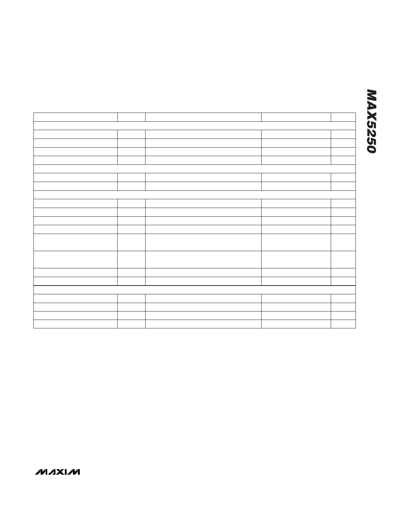
ELECTRICAL CHARACTERISTICS (continued)
(VDD = +5V ±10%, AGND = DGND = 0V, REFAB = REFCD = 2.5V, RL = 5kΩ, CL = 100pF, TA = TMIN to TMAX, unless otherwise
noted. Typical values are at TA = +25°C. Output buffer connected in unity-gain configuration (Figure 9).)
PARAMETER
SYMBOL
CONDITIONS
MIN TYP MAX UNITS
DIGITAL INPUTS
Input High Voltage
Input Low Voltage
Input Leakage Current
Input Capacitance
DIGITAL OUTPUTS
VIH
VIL
IIN
VIN = 0V or VDD
CIN
2.4
V
0.8
V
0.01 ±1.0 µA
8
pF
Output High Voltage
Output Low Voltage
DYNAMIC PERFORMANCE
VOH
VOL
ISOURCE = 2mA
ISINK = 2mA
VDD - 0.5
V
0.13
0.4
V
Voltage Output Slew Rate
SR
0.6
V/µs
Output Settling Time
Output Voltage Swing
Current into FB_
To ±1/2LSB, VSTEP = 2.5V
Rail-to-rail (Note 2)
10
µs
0 to VDD
V
0
0.1
µA
OUT_ Leakage Current
in Shutdown
RL = ∞
0.01
±1
µA
Start-Up Time Exiting
Shutdown Mode
Digital Feedthrough
Digital Crosstalk
CS = VDD, DIN = 100kHz
POWER SUPPLIES
Supply Voltage
Supply Current
Supply Current in Shutdown
VDD
IDD (Note 3)
(Note 3)
Reference Current in Shutdown
15
µs
5
nV-s
5
nV-s
4.5
5.5
V
0.85 0.98 mA
10
20
µA
0.01
±1
µA
Note 1: Guaranteed from code 3 to code 1023 in unity-gain configuration.
Note 2: Accuracy is better than 1LSB for VOUT = 6mV to VDD - 60mV, guaranteed by a power-supply rejection test at the
end points.
Note 3: RL = ∞, digital inputs at DGND or VDD.
_______________________________________________________________________________________ 3
Share Link: