IDT74FST163209 Просмотр технического описания (PDF) - Integrated Device Technology
Номер в каталоге
Компоненты Описание
Список матч
IDT74FST163209 Datasheet PDF : 6 Pages
| |||
IDT74FST163209
9-BIT BUS EXCHANGE SWITCH
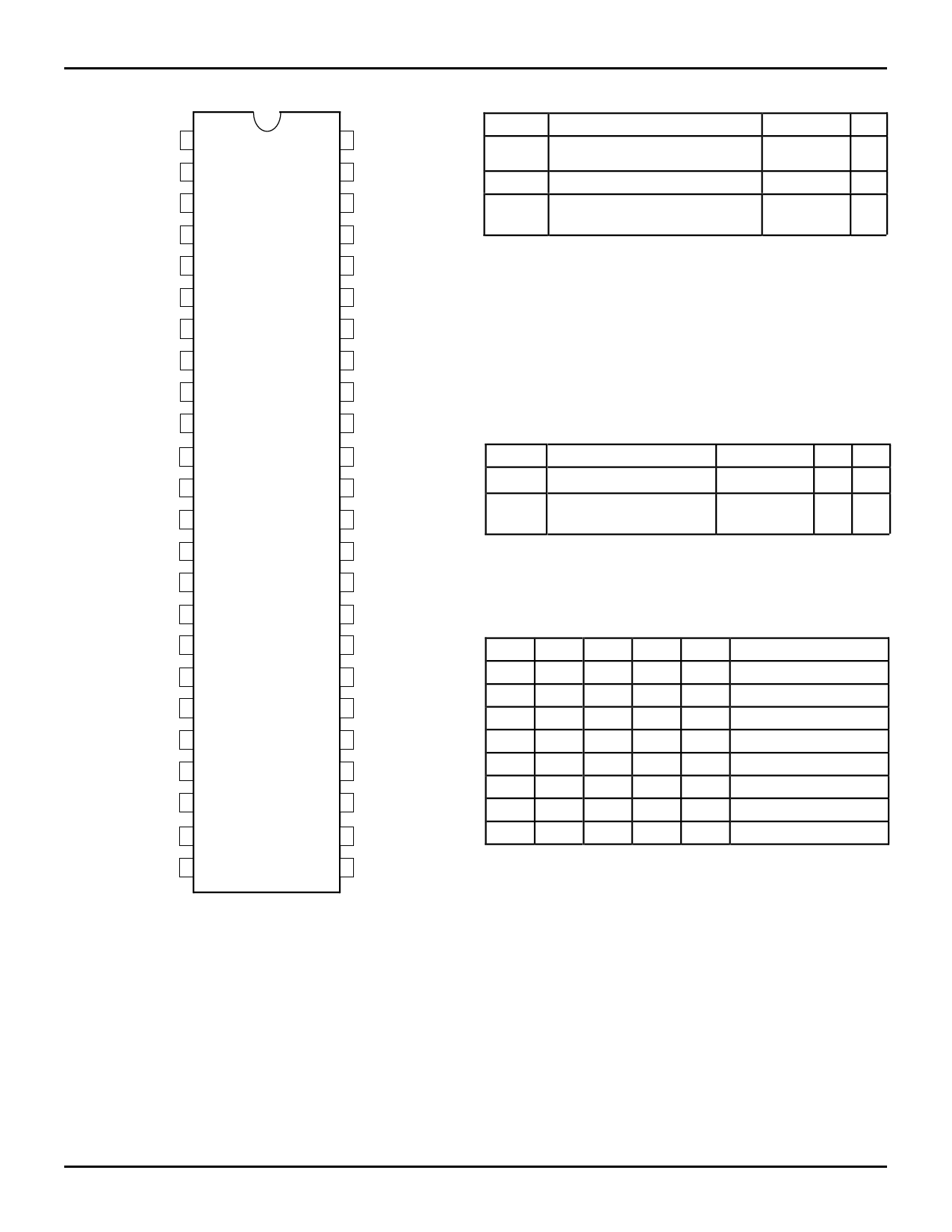
PIN CONFIGURATION
S0 1
1A1
2
1A2 3
GND 4
2A1 5
2A2 6
VCC 7
3A1 8
3A2 9
GND 10
48 S1
47 S2
46 1B1
45 1B2
44 2B1
43 2B2
42 GND
41 3B1
40 3B2
39 GND
4A1 11
38 4B1
4A2 12 SO48-1
37
4B2
SO48-2
5A1 13 SO48-3
36
5B1
5A2 14
35 5B2
GND 15
34 GND
6A1 16
33 6B1
6A2 17
32 6B2
7A1 18
31 7B1
7A2 19
30 7B2
GND 20
29 GND
8A1 21
8A2 22
28 8B1
27 8B2
9A1 23
9A2 24
26 9B1
25 9B2
SSOP/
TSSOP/TVSOP
TOP VIEW
3510 drw 02
COMMERCIAL TEMPERATURE RANGE
ABSOLUTE MAXIMUM RATINGS(1)
Symbol
Description
VTERM(2) Terminal Voltage with Respect
to GND
TSTG
Storage Temperature
Max. Unit
–0.5 to +7.0 V
–65 to +150 °C
IOUT
Maximum Continuous Channel
Current
128
mA
NOTES:
3510 tbl 02
1. Stresses greater than those listed under ABSOLUTE MAXIMUM RAT-
INGS may cause permanent damage to the device. This is a stress rating
only and functional operation of the device at these or any other conditions
above those indicated in the operational sections of this specification is
not implied. Exposure to absolute maximum rating condiitions for ex-
tended periods may affect reliability.
2. VCC, Control and Switch terminals.
CAPACITANCE(1)
Symbol
Parameter
Conditions(2) Typ. Unit
CIN
Control Input Capacitance
4 pF
CI/O
Switch Input/Output
Capacitance
Switch Off
NOTES:
1. Capacitance is characterized but not tested
2. TA = 25°C, f = 1MHz, VIN = 0V, VOUT = 0V
pF
3510 tbl 03
FUNCTION TABLE
S2
S1
S0
A1
A2
L
L
L
Z
Z
L
L
H
B1
Z
L
H
L
B2
Z
L
H
H
Z
B1
H
L
L
Z
B2
H
L
H
Z
Z
H
H
L
B1
B2
H
H
H
B2
B1
Function
Disconnect
A1 to B1
A1 to B2
A2 to B1
A2 to B2
Disconnect
A1 to B1, A2 to B2
A1 to B2, A2 to B1
3510 tbl 04
2
Share Link: 