HMC500LP3(V02) Просмотр технического описания (PDF) - Hittite Microwave
Номер в каталоге
Компоненты Описание
Список матч
HMC500LP3 Datasheet PDF : 8 Pages
| |||
v02.1109
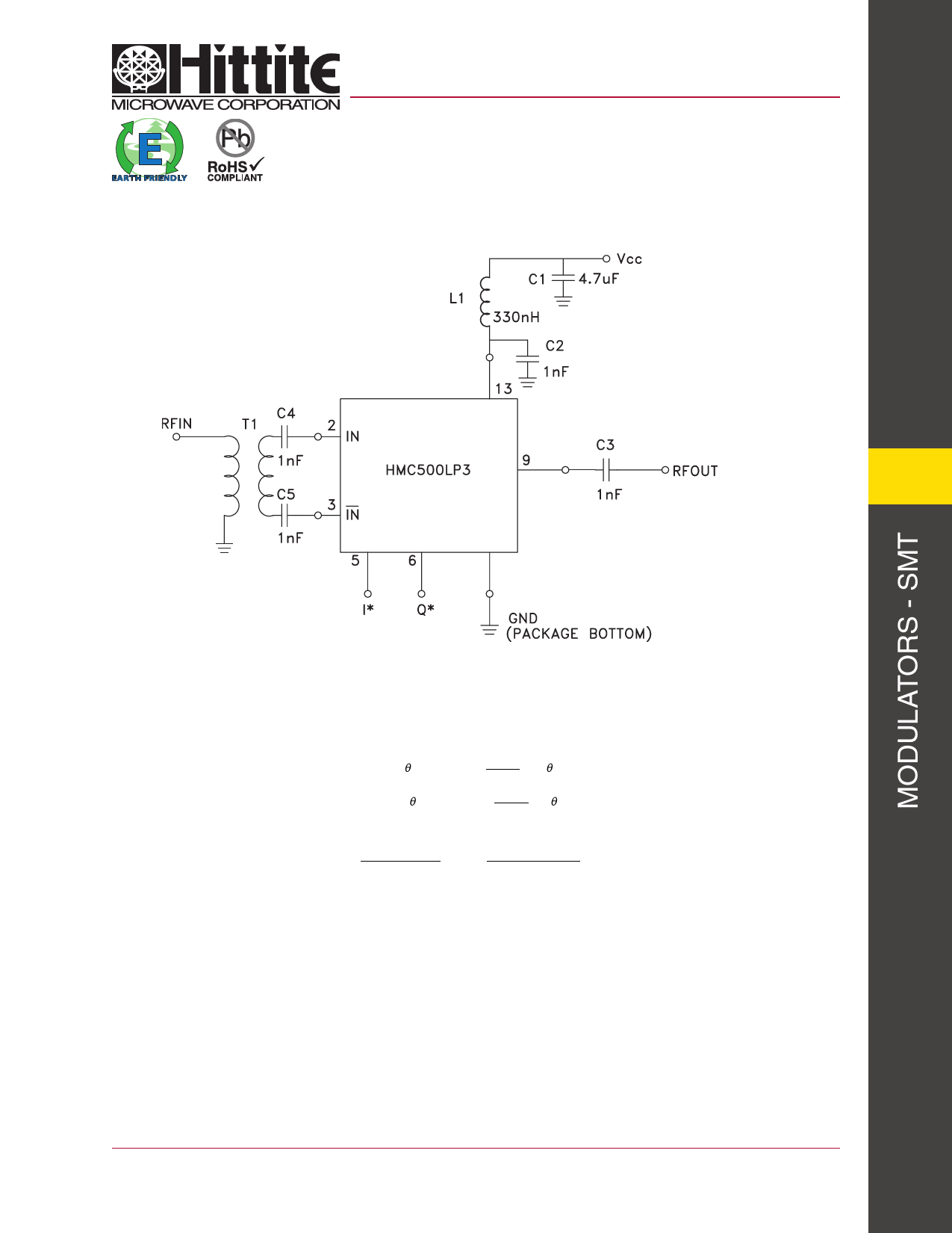
Application Circuit
HMC500LP3 / 500LP3E
GaAs HBT VECTOR
MODULATOR 1.8 - 2.2 GHz
10
* Pins 15 & 16 are redundant I & Q inputs.
Gain and Phase control are applied through the I and Q control ports. For a given linear gain (G) and phase () setting, the
voltages applied to these ports in all measurements are calculated as follows:
I(G,θ ) = Vmi + 1.0V G Cos(θ )
G max
Q(G,θ ) = Vmq + 1.0V G Sin(θ )
G max
Where Vmi and Vmq are the I and Q voltage settings corresponding to maximum isolation at room temperature and F = 2 GHz.
Note that G=10X and Gmax = 10Y where x = Gain Setting ( dB) and y = Max Gain Setting( dB) . Nominally Vmi = Vmq = 1.5V, Gmax = 0.316.
20
20
For price, delivery, and to place orders, please contact Hittite Microwave Corporation:
20 Alpha Road, Chelmsford, MA 01824 Phone: 978-250-3343 Fax: 978-250-3373
Order On-line at www.hittite.com
10 - 39
Share Link: 