HFBR-5103A Просмотр технического описания (PDF) - HP => Agilent Technologies
Номер в каталоге
Компоненты Описание
Список матч
HFBR-5103A
HP => Agilent Technologies

HFBR-5103A Datasheet PDF : 21 Pages
| |||
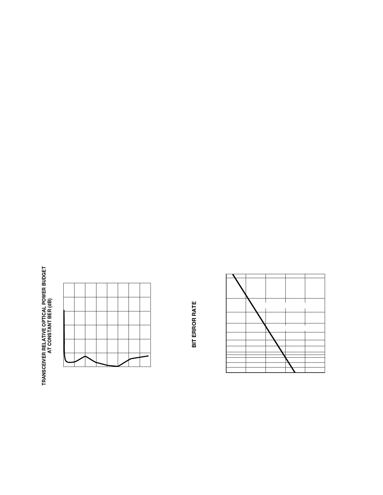
These transceivers can also be
used for applications which
require different Bit Error Rate
(BER) performance. Figure 6
illustrates the typical trade-off
between link BER and the
receivers input optical power
level.
Transceiver Jitter Performance
The Agilent 1300 nm transceivers
are designed to operate per the
system jitter allocations stated in
Tables E1 of Annexes E of the
FDDI PMD and LCF-PMD
standards.
The Agilent 1300 nm transmitters
will tolerate the worst case input
electrical jitter allowed in these
tables without violating the worst
case output jitter requirements of
Sections 8.1 Active Output
Interface of the FDDI PMD and
LCF-PMD standards.
The Agilent 1300 nm receivers will
tolerate the worst case input
optical jitter allowed in Sections
8.2 Active Input Interface of the
FDDI PMD and LCF-PMD
standards without violating the
worst case output electrical jitter
allowed in the Tables E1 of the
Annexes E.
The jitter specifications stated in
the following 1300 nm transceiver
specification tables are derived
from the values in Tables E1 of
Annexes E. They represent the
worst case jitter contribution that
the transceivers are allowed to
make to the overall system jitter
without violating the Annex E
allocation example. In practice
the typical contribution of the
Agilent transceivers is well below
these maximum allowed amounts.
Recommended Handling Precautions
Agilent recommends that normal
static precautions be taken in the
handling and assembly of these
transceivers to prevent damage
which may be induced by
electrostatic discharge (ESD). The
HFBR-5100 series of transceivers
meet MIL-STD-883C Method
3015.4 Class 2 products.
Care should be used to avoid
shorting the receiver data or signal
detect outputs directly to ground
without proper current limiting
impedance.
3.0
2.5
2.0
1.5
1.0
0.5
0
0 25 50 75 100 125 150 175 200
SIGNAL RATE (MBd)
CONDITIONS:
1. PRBS 27-1
2. DATA SAMPLED AT CENTER OF DATA SYMBOL.
3. BER = 10-6
4. TA = 25° C
5. VCC = 5 Vdc
6. INPUT OPTICAL RISE/FALL TIMES = 1.0/2.1 ns.
Figure 5. Transceiver Relative Optical Power Budget at Constant
BER vs. Signaling Rate.
1 x 10⁻²
1 x 10⁻³
1 x 10⁻⁴
HFBR-5103/5103T SERIES
1 x 10⁻⁵
1 x 10⁻⁶
1 x 10⁻⁷
1 x 10⁻⁸
2.5 x 10⁻¹⁰
1 x 10-11
1 x 10-12
-6 -4
CENTER OF SYMBOL
-2
0
2
4
RELATIVE INPUT OPTICAL POWER – dB
CONDITIONS:
1. 125 MBd
2. PRBS 27-1
3. CENTER OF SYMBOL SAMPLING.
4. TA = 25° C
5. VCC = 5 Vdc
6. INPUT OPTICAL RISE/FALL TIMES = 1.0/2.1 ns.
Figure 6. Bit Error Rate vs. Relative Receiver Input Optical
Power.
7
Share Link: