GF9103 Просмотр технического описания (PDF) - Gennum -> Semtech
Номер в каталоге
Компоненты Описание
Список матч
GF9103 Datasheet PDF : 9 Pages
| |||
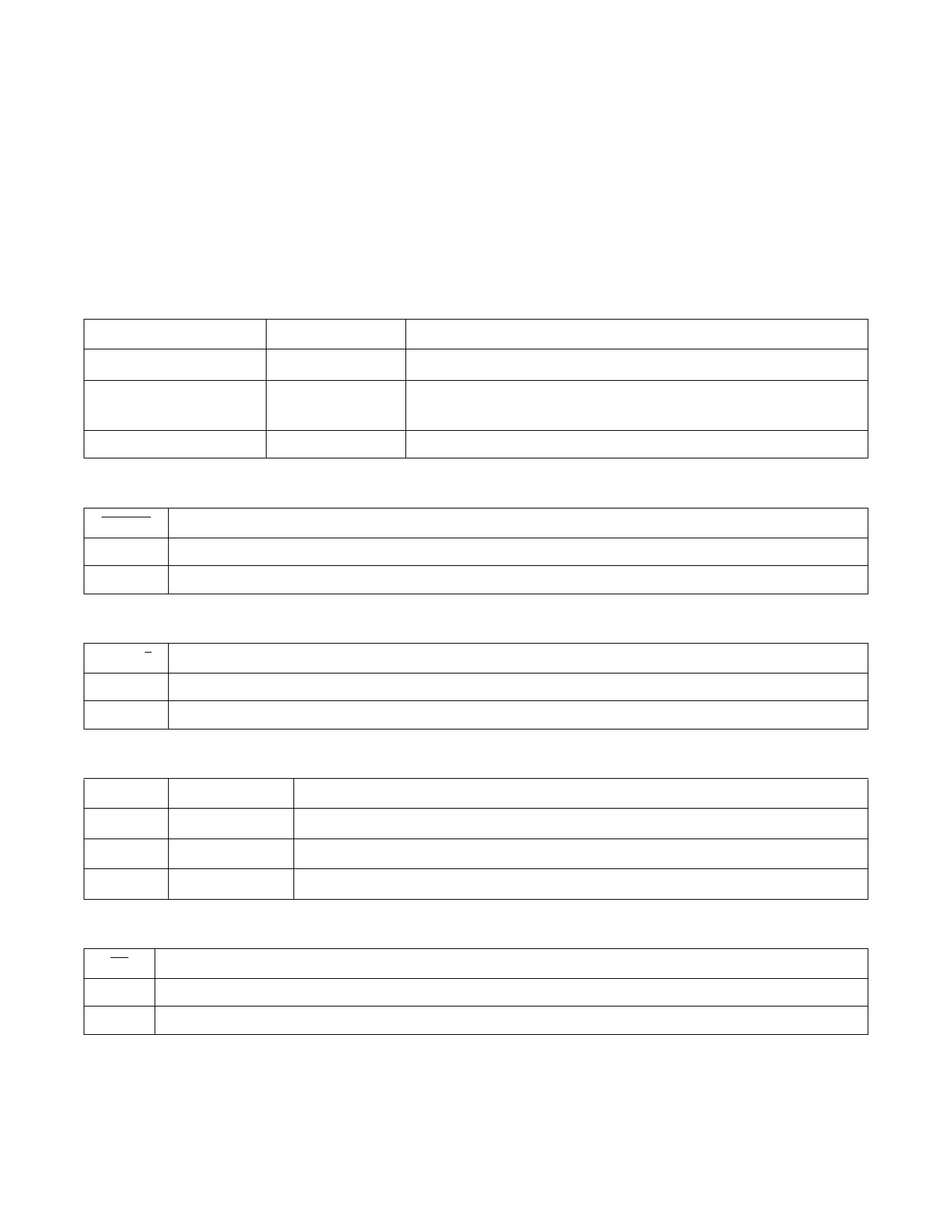
CONTROL SIGNAL/OPERATING MODE SUMMARY
SYNC
The SYNC control signal provides synchronization for the internal 4:2:2 de-multiplexer. SYNC should be held high on clock
period N and low on clock period N+1 when the first CB sample is presented to the SI9..0 inputs. SYNC may be held low until
re-synchronization is desired or may be toggled at every occurrence of a CB sample.
SELECT_MATRIX AND SETUP
SELECT_MATRIX and SETUP select the color space conversion and offset insertions which the GF9103 is to perform. The
following chart presents the available color space conversions and the corresponding states of the SELECT_MATRIX and
SETUP control pins. SETUP is a dynamic pin that may be modified every clock cycle.
SELECT_MATRIX
0
0
1
SETUP
0
1
X
DESCRIPTION
Selects output to be over-sampled YCBCR with no setup in Y channel.
Selects output to be over-sampled YCBCR with a scaling factor of
+947/1024 and an offset of +71 (decimal) applied to the Y channel.
Selects output to be over-sampled RGB with no setup.
SIN X/X CORRECTION
BYPASS
DESCRIPTION
1
SIN X/X correction enabled on all output data channels. Latency through the device is 24 clock cycles.
0
SIN X/X correction disabled. Latency through the device is 22 clock cycles.
OUTPUT ROUNDING
RND10/8
DESCRIPTION
1
Output data rounded to 10 bit resolution per channel.
0
Output data rounded to 8 bit resolution per channel.
TWO’S COMPLEMENT OUTPUT CONVERSION
CONVERT SELECT_MATRIX
DESCRIPTION
1
0
SOB9..0 and SOC9..0 output signed (two's complement) CB and CR data.
0
0
SOB9..0 and SOC9..0 output unsigned (offset binary) CB and CR data.
X
1
SOB9..0 and SOC9..0 output unsigned B and R data.
OUTPUT ENABLE
OE
0
All output data ports are enabled.
1
All output data ports are in high impedance state.
DESCRIPTION
5
521 - 33 - 04
Share Link: 