G9131 Просмотр технического описания (PDF) - Global Mixed-mode Technology Inc
Номер в каталоге
Компоненты Описание
Список матч
G9131 Datasheet PDF : 10 Pages
| |||
Global Mixed-mode Technology Inc.
G9131
Absolute Maximum Ratings
(Note 1)
Input Voltage.............................................................7V
Power Dissipation Internally Limited
(Note2)
Maximum Junction Temperature.........................150°C
Storage Temperature Range.........-65°C ≤ TJ ≤+150°C
Reflow Temperature (soldering, 10sec) ...........260°C
Thermal Resistance Junction to Ambient, (θJA)
SOT-23(1) .......................................................276°C/W
SOT-89(1) ......................................... .............173°C/W
Thermal Resistance Junction to Case, (θJC)
SOT-89......................... ................................. .24°C/W
Operating Conditions
(Note 1)
Input Voltage.......................... ...........................3V ~ 6V
Temperature Range...........................-40°C ≤ TA ≤85°C
Note (1): See Recommended Minimum Footprint.
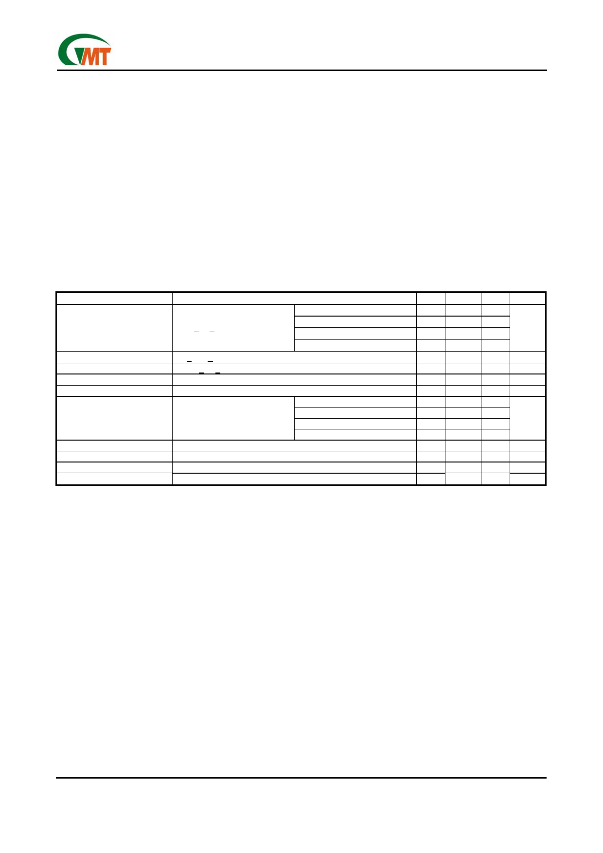
Electrical Characteristics
VIN =5V, IO = 300mA, CIN=1µF, COUT =1µF. All specifications apply for TA = TJ = 25°C. [Note 3]
PARAMETER
Output Voltage
Line Regulation
Load Regulation
Quiescent Current
Ripple Rejection
Dropout Voltage
Short Circuit Current
Current Limit
Over Temperature
Over Temperature Hysterics
CONDITION
VO=3.3V
5mA < IO < 300mA
VO=2.5V
VO=1.8V
VO=1.5V
4V < VIN < 6V, IO = 10mA
10mA < IO < 300mA
VIN = 5V
fi = 120 Hz, 1VP-P, Io = 100mA
IO = 300mA
VO=3.3V
VO=2.5V
VO=1.8V
VO=1.5V
MIN
3.234
2.45
1.764
1.455
---
---
---
---
---
---
---
---
---
---
---
---
TYP
3.3
2.5
1.8
1.5
15
10
90
45
0.4
0.5
0.8
0.9
0.65
0.8
145
25
MAX
3.366
2.55
1.845
1.545
---
---
150
---
---
---
---
---
---
---
---
---
UNIT
V
mV
mV
µA
dB
V
A
A
°C
°C
Note 1:
Note2:
Note3:
Note4:
Absolute Maximum Ratings are limits beyond which damage to the device may occur. Operating Conditions are condi-
tions under which the device functions but the specifications might not be guaranteed. For guaranteed specifications and
test conditions see the Electrical Characteristics.
The maximum power dissipation is a function of the maximum junction temperature, TJmax ; total thermal resistance, θJA,
and ambient temperature TA. The maximum allowable power dissipation at any ambient temperature is Tjmax-TA / θJA. If this
dissipation is exceeded, the die temperature will rise above 150°C and IC will go into thermal shutdown. For the G9131 in
SOT-23 package, θJA is 276°C/W and in the SOT-89 package is 173°C/W (See Recommended Minimum Footprint). The
safe operation in SOT-89 & SOT-23 package, it can see “Typical Performance Characteristics” (Safe Operating Area).
Low duty pulse techniques are used during test to maintain junction temperature as close to ambient as possible.
The type of output capacitor should be tantalum, aluminum or ceramic.
Ver: 1.6
Dec 22, 2005
TEL: 886-3-5788833
http://www.gmt.com.tw
2
Share Link: 