DCR1003SF14 Просмотр технического описания (PDF) - Dynex Semiconductor
Номер в каталоге
Компоненты Описание
Список матч
DCR1003SF14 Datasheet PDF : 8 Pages
| |||
DCR1003SF
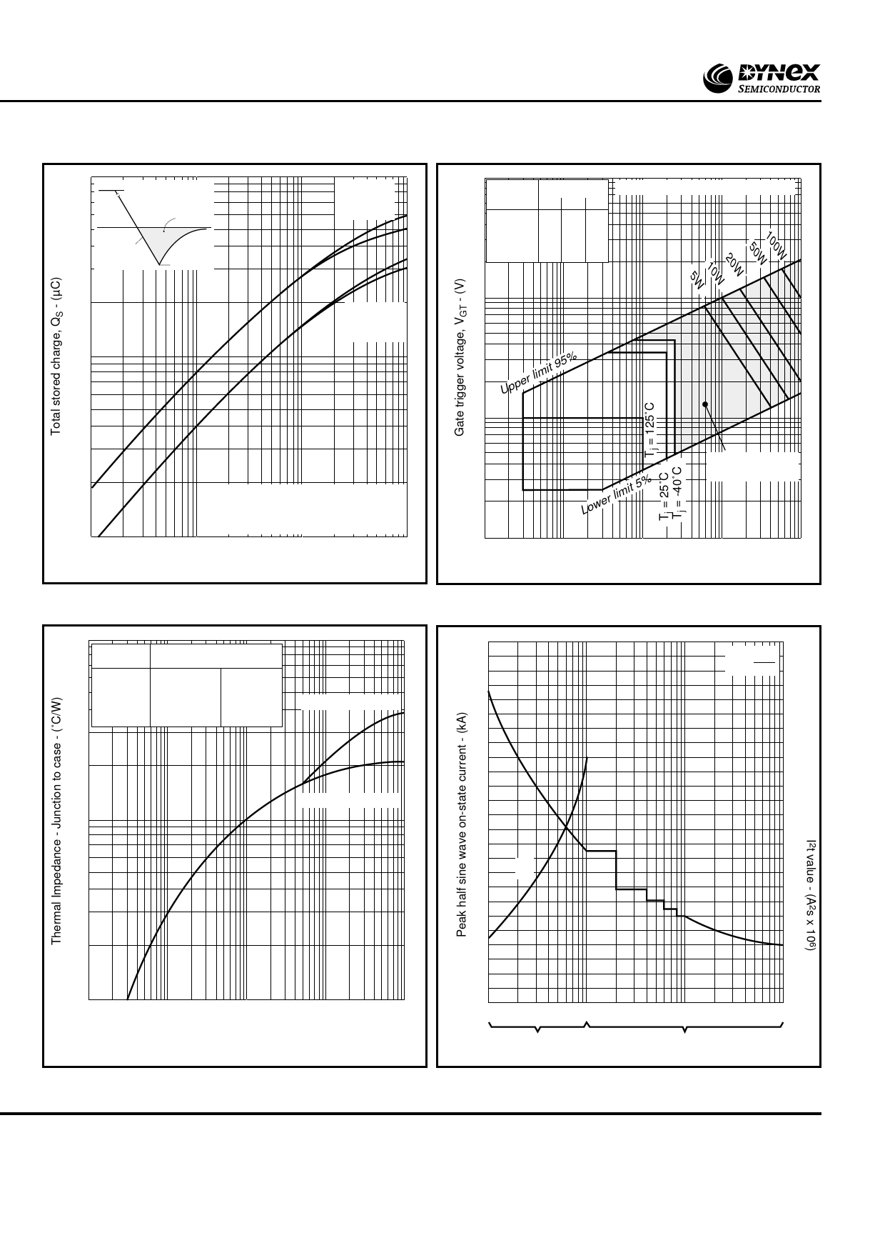
10000
IT
QS
dI/dt
IRR
1000
IT = 2000A
IT = 1000A
Max. value
IT = 2000A
IT = 1000A
Min. value
100
0.1
Conditions:
QS is total integral stored charge
Tj = 125˚C
1.0
10
100
Rate of decay of on-state current, dI/dt - (A/µs)
Fig.4 Stored charge
0.1
Conduction
d.c.
Halfwave
3 phase 120˚
6 phase 60˚
Effective thermal resistance
Junction to case ˚C/W
Double side
0.022
0.024
0.026
0.027
Anode side
0.038
0.040
0.042
0.043
Anode side cooled
100
Pulse width Frequency Hz
µs
50 100 400
100 150 150 150
200 150 150 125
500 150 150 100
1ms 150 50 25
10ms 20 - -
Table gives pulse power PGM in Watts
10
Upper limit 95%
1
VGD
0.1
0.001
Lower limit 5%
Region of certain
triggering
0.01
0.1
1
10
Gate trigger current, IGT - (A)
Fig.5 Gate characteristics
50
I2t = Î2 x t
2
40
30
2.0
Double side cooled
0.01
20
1.5
I2t
10
1.0
0.001
0.001
0.01
0.1
1.0
10
Time - (s)
Fig.6 Transient thermal impedance - junction to case
0
0.5
1
10 1 2 3 45 10 20 30 50
ms
Cycles at 50Hz
Duration
Fig.7 Surge (non-repetitive) on-state current vs time (with
50% VRRM at Tcase = 125˚C)
6/8
www.dynexsemi.com
Share Link: 