ACT-SF128K32 Просмотр технического описания (PDF) - Aeroflex Corporation
Номер в каталоге
Компоненты Описание
Список матч
ACT-SF128K32 Datasheet PDF : 10 Pages
| |||
ACT-SF128K32 High Speed
128Kx32 SRAM / 128Kx32 Flash
Multichip Module
FEATURES
s 4 – 128K x 8 SRAMs & 4 – 128K x 8 Flash Die
in One MCM
s Access Times of 25ns (SRAM) and 60ns
(Flash) or 35ns (SRAM) and 70ns or
90ns (Flash)
s Organized as 128K x 32 of SRAM and 128K x
32 of Flash Memory with Common Data Bus
s Low Power CMOS
s Input and Output TTL Compatible Design
s MIL-PRF-38534 Compliant MCMs Available
s Decoupling Capacitors and Multiple
Grounds for Low Noise
s Commercial, Industrial and Military
Temperature Ranges
s Industry Standard Pinouts
s TTL Compatible Inputs and Outputs
s Packaging – Hermetic Ceramic
q 66–Lead, PGA-Type, 1.385"SQ x 0.245"max,
Aeroflex code# P3,P7 without/with shoulders
CIRCUIT TECHNOLOGY
www.aeroflex.com
FLASH MEMORY FEATURES
s Sector Architecture (Each Die)
q 8 Equal Sectors of 16K bytes each
q Any combination of sectors can be erased with
one command sequence.
s +5V Programing, +5V Supply
s Embedded Erase and Program Algorithms
s Hardware and Software Write Protection
s Page Program Operation and Internal
Program Control Time.
s 10,000 Erase/Program Cycles
FLEX LAB
ISO
9001
CE R T I F I E D
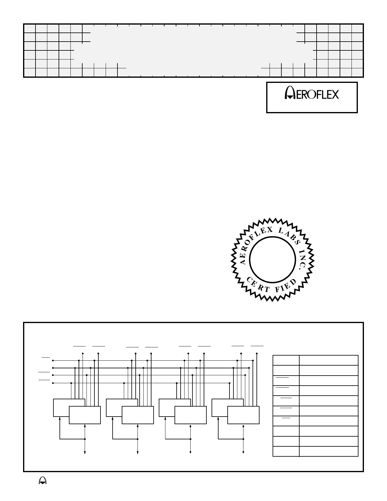
Block Diagram – PGA Type Package (P3 & P7)
OE
A0–A16
SCE
FCS
FWE1 SWE1
FWE2 SWE2
FWE3 SWE3
FWE4 SWE4
128K X 8 FLASH
128K X 8 SRAM
128K X 8 FLASH
128K X 8 SRAM
128K X 8 FLASH
128K X 8 SRAM
128K X 8 FLASH
128K X 8 SRAM
I/O0-7
I/O8-15
I/O16-23
I/O24-31
PIN DESCRIPTION
I/O0-31
Data I/O
A0–16
Address Inputs
FWE1-4 Flash Write Enables
SWE1-4 SRAM Write Enables
FCE Flash Chip Enable
SCE SRAM Chip Enable
OE
Output Enable
NC
Not Connected
VCC
Power Supply
GND
Ground
eroflex Circuit Technology - Advanced Multichip Modules © SCD3850 REV A 5/20/98
Share Link: 