74F30 Просмотр технического описания (PDF) - Philips Electronics
Номер в каталоге
Компоненты Описание
Список матч
74F30 Datasheet PDF : 8 Pages
| |||
Philips Semiconductors
8-input NAND gate
Product specification
74F30
DC ELECTRICAL CHARACTERISTICS
(Over recommended operating free-air temperature range unless otherwise noted.)
SYMBOL
PARAMETER
TEST CONDITIONS1
LIMITS
MIN TYP2 MAX
UNIT
VOH
High-level output voltage
VCC = MIN, VIL = MAX
±10%VCC
2.5
V
VIH = MIN, IOH = MAX
±5%VCC
2.7
3.4
VOL
Low-level output voltage
VCC = MIN, VIL = MAX
VIH = MIN, IOL = MAX
±10%VCC
±5%VCC
0.30 0.50
V
0.30 0.50
VIK
Input clamp voltage
VCC = MIN, II = IIK
–0.73 –1.2
V
II
Input current at maximum input voltage
VCC = MAX, VI = 7.0V
100
µA
IIH
High-level input current
VCC = MAX, VI = 2.7V
20
µA
IIL
Low-level input current
IOS
Short-circuit output current3
VCC = MAX, VI = 0.5V
VCC = MAX
–0.6
mA
–60
–150
mA
ICC
Supply current (total)
ICCH VCC = MAX
ICCL
VIN = GND
VIN = 4.5V
0.6
1.5
mA
2.8
4.0
NOTES:
1. For conditions shown as MIN or MAX, use the appropriate value specified under recommended operating conditions for the applicable type.
2. All typical values are at VCC = 5V, Tamb = 25°C.
3. Not more than one output should be shorted at a time. For testing IOS, the use of high-speed test apparatus and/or sample-and-hold
techniques are preferable in order to minimize internal heating and more accurately reflect operational values. Otherwise, prolonged shorting
of a High output may raise the chip temperature well above normal and thereby cause invalid readings in other parameter tests. In any
sequence of parameter tests, IOS tests should be performed last.
AC ELECTRICAL CHARACTERISTICS
SYMBOL
PARAMETER
tPLH
Propagation delay
tPHL
Da, Db, Dc, Dd, De, Df, Dg, Dh to Q
TEST
CONDITION
Waveform 1
LIMITS
VCC = +5.0V
Tamb = +25°C
CL = 50pF, RL = 500Ω
MIN
TYP MAX
VCC = +5.0V ± 10%
Tamb = 0°C to +70°C
CL = 50pF, RL = 500Ω
MIN
MAX
1.5
3.5
5.0
1.5
5.5
1.0
3.0
4.5
1.0
5.0
UNIT
ns
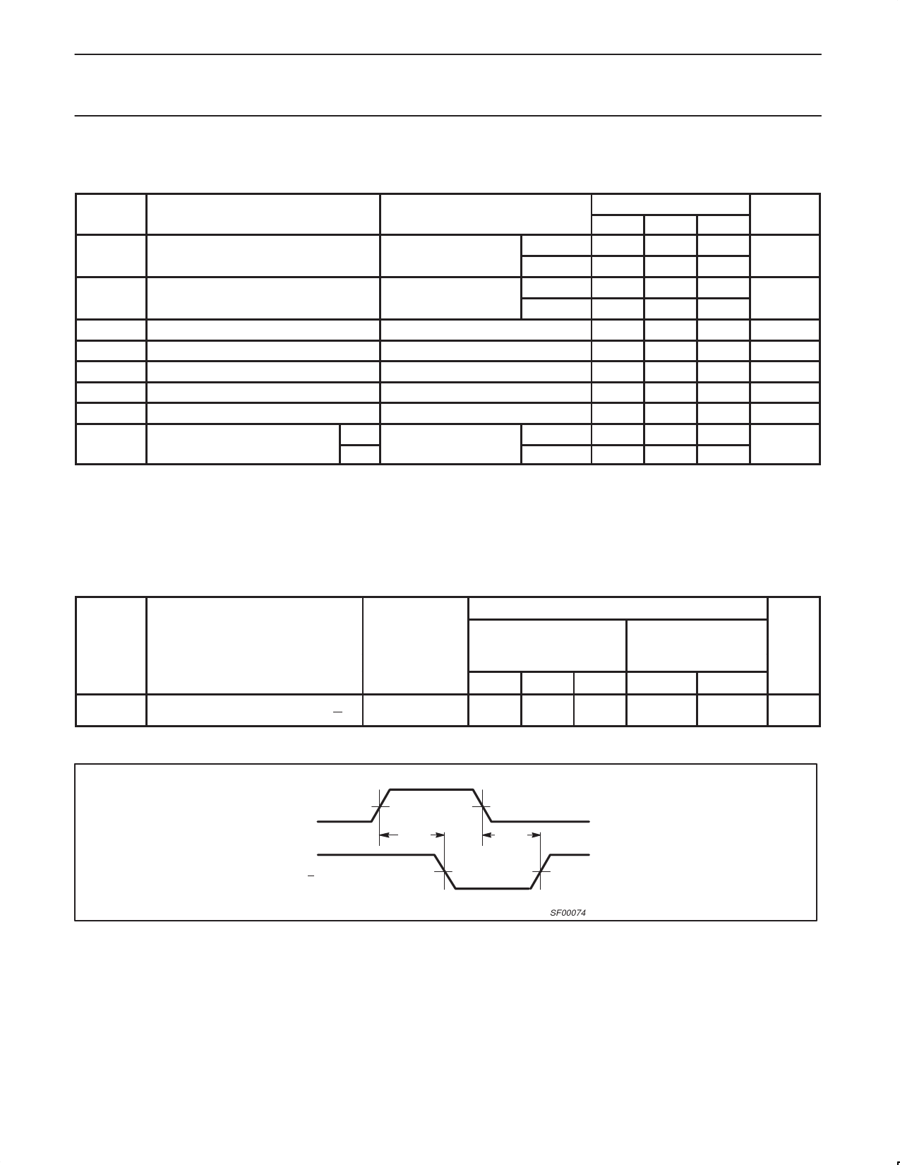
AC WAVEFORMS
Da, Db, Dc, Dd,
De, Df, Dg, Dh
VM
VM
tPHL
tPLH
NOTE:
For all waveforms, VM = 1.5V.
Q
VM
VM
SF00074
Waveform 1. Propagation Delay for Inverting Outputs
March 3, 1989
4
Share Link: 