TLP651 Просмотр технического описания (PDF) - Toshiba
Номер в каталоге
Компоненты Описание
Список матч
TLP651 Datasheet PDF : 7 Pages
| |||
TLP651
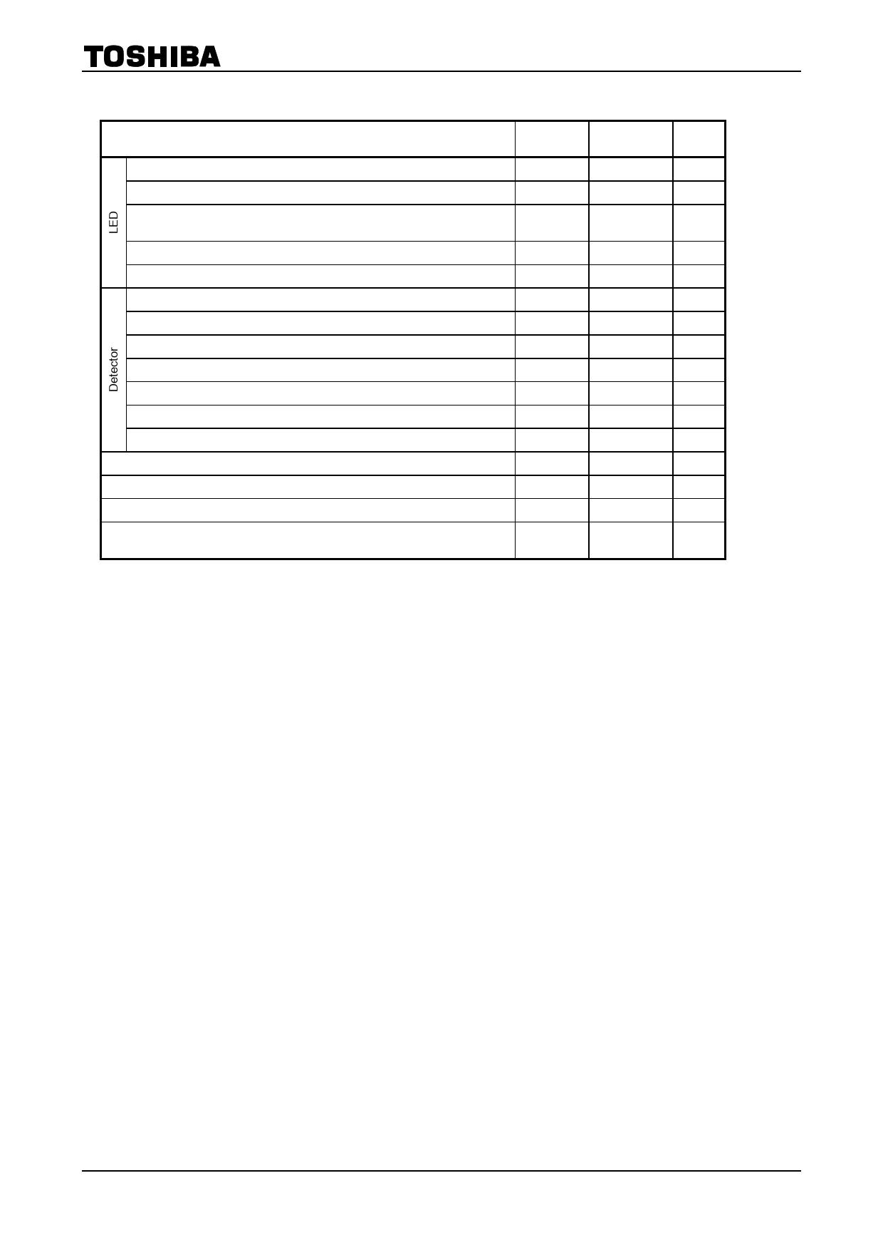
Absolute Maximum Ratings (Ta = 25°C)
Characteristic
Symbol
Rating
Unit
Forward current
Pulse forward current
Peak transient forward
current
Reverse voltage
Diode power dissipation
Output current
Peak output current
Output voltage
Supply voltage
Base current
Emitter−base reverse voltage
Output power dissipation
Operating temperature range
Storage temperature range
Lead solder temperature (10s)
Isolation voltage
(AC, 1min., R.H.≤ 60%)
(Note 1)
(Note 2)
(Note 3)
(Note 4)
(Note 5)
(Note 6)
(Note 7)
IF
IFP
IFPT
VR
PD
IO
IOP
VO
VCC
IB
VEB
PO
Topr
Tstg
Tsol
BVS
25
50
1
5
45
8
16
−0.5~15
−0.5~15
5
5
100
−55~100
−55~125
260
5000
mA
mA
A
V
mW
mA
mA
V
V
mA
V
mW
°C
°C
°C
Vrms
Note: Using continuously under heavy loads (e.g. the application of high temperature/current/voltage and the
significant change in temperature, etc.) may cause this product to decrease in the reliability significantly even
if the operating conditions (i.e. operating temperature/current/voltage, etc.) are within the absolute maximum
ratings.
Please design the appropriate reliability upon reviewing the Toshiba Semiconductor Reliability Handbook
(“Handling Precautions”/“Derating Concept and Methods”) and individual reliability data (i.e. reliability test
report and estimated failure rate, etc).
(Note 1) Derate 0.8mA above 70°C.
(Note 2) 50% duty cycle,1ms pulse width.
Derate 1.6mA / °C above 70°C.
(Note 3) Pulse width ≤ 1μs, 300pps.
(Note 4) Derate 0.9mW / °C above 70°C.
(Note 5) Derate 2mW / °C above 70°C.
(Note 6) Soldering portion of lead: Up to 2mm from the body of the device.
(Note 7) Device considered a two terminal device: Pins 1, 2, 3 and 4 shorted together and pins 5, 6, 7 and 8 shorted
together.
2
2007-10-01
Share Link: 