OZ960 Просмотр технического описания (PDF) - O2Micro International
Номер в каталоге
Компоненты Описание
Список матч
OZ960 Datasheet PDF : 12 Pages
| |||
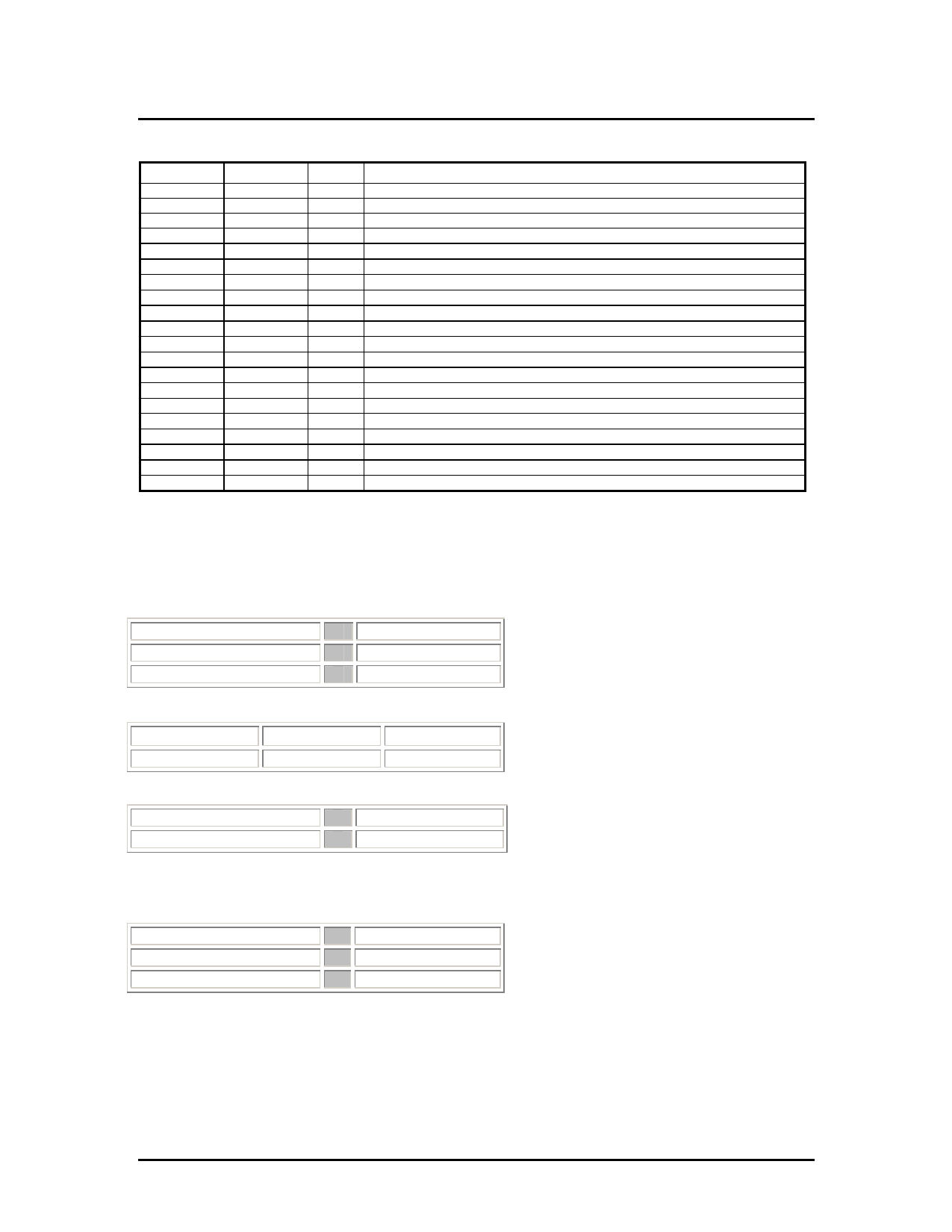
PIN DESCRIPTION
OZ960
Names
CTIMR
OVP
ENA
SST
VDDA
GNDA
REF
RT1
FB
CMP
NDR_D
PDR_C
LPWM
DIM
LCT
PGND
RT
CT
PDR_A
NDR_B
Pin No.
1
2
3
4
5
6
7
8
9
10
11
12
13
14
15
16
17
18
19
20
I/O
Description
I
Capacitor for CCFL ignition duration
I
Output voltage sense Vth=2.0V
I
Enable input; TTL signal is applicable
I
Soft-start capacitor
I
Voltage source for the IC
I
Analog signal ground reference
O Reference voltage output; 2.5V typical
I
Resistor for programming ignition frequency
I
CCFL current feedback signal
O Compensation output of the current error amplifier
O NMOSFET drive output
O PMOSFET drive output
O Low-frequency PWM signal for burst-mode dimming control
I
Input analog signal for burst-mode dimming control
I
Triangular wave for burst-mode dimming; frequency
I
Power ground reference
I
Timing resistor set operating frequency
I
Timing capacitor set operating frequency
O PMOSFET drive output
O NMOSFET drive output
ABSOLUTE MAXIMUM RATINGS WITH
RESPECT TO INPUT POWER SOURCE
RETURN REFERENCE
VDDA
GNDA, PGND
Logic inputs
7.0V(1)
+/- 0.3V
-0.3V to VDD +0.3V
Operating temp.
OZ960
0oC to 70oC
OZ960I
-40oC to 85oC
Operating junction temp.
Storage temp.
150 oC
-55 oC to 150 oC
RECOMMENDED OPERATING RANGE
VDDA
Fosc
Rosc
4.7V ~ 5.5V
30 KHz to 150 KHz
50 k to 150 k
Note (1): The “Absolute Maximum Ratings” are those values beyond which the safety of the device cannot be guaranteed.
The device should not be operated at these limits. The “Functional Specifications” table will define the conditions for
actual device operation. Exposure to absolute maximum rated conditions for extended periods may affect device
reliability.
OZ960-DS-1.6
Page 4
Share Link: 