UCS1903 Просмотр технического описания (PDF) - Unspecified
Номер в каталоге
Компоненты Описание
Список матч
UCS1903 Datasheet PDF : 9 Pages
| |||

UCS1903
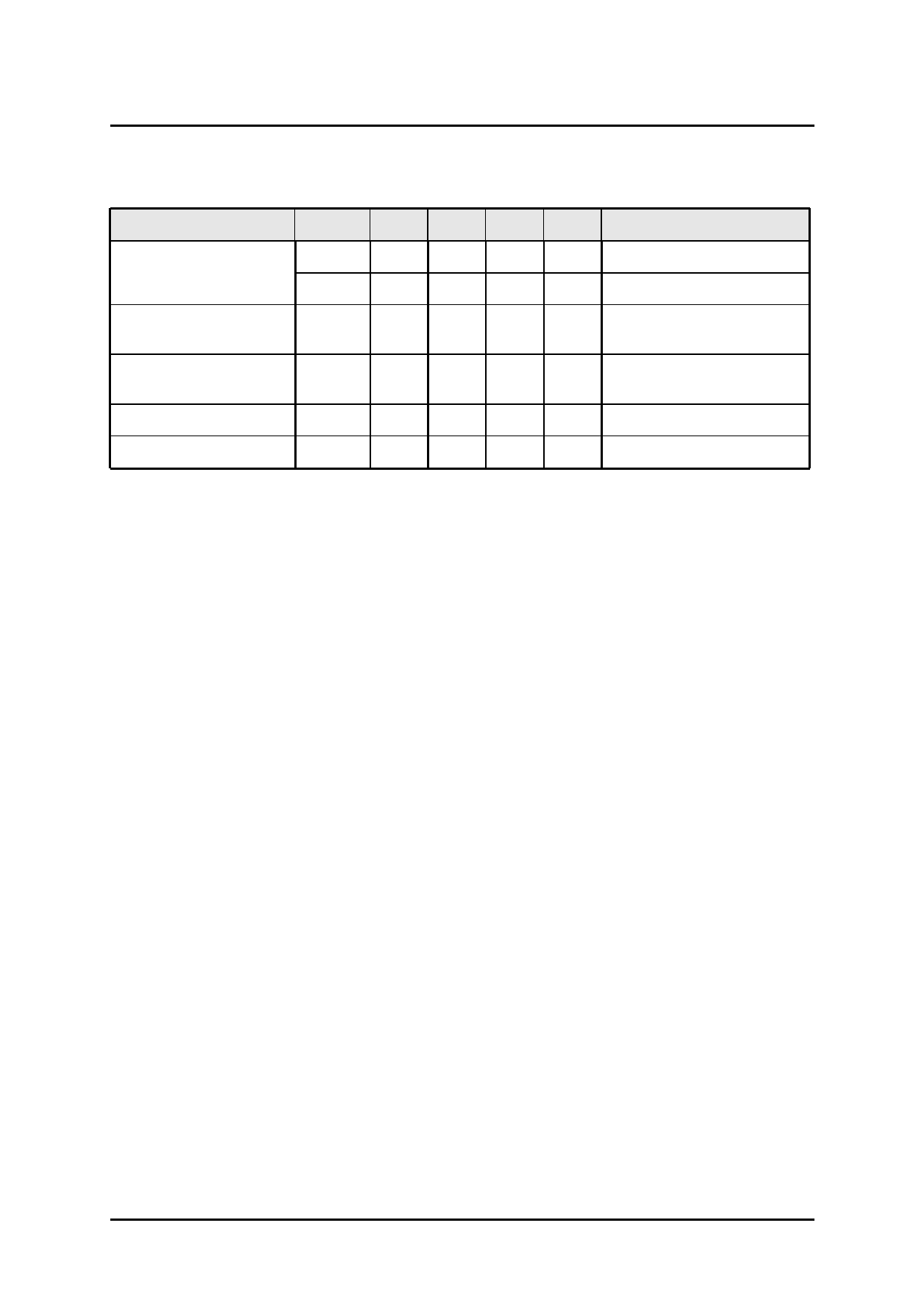
SWITCHING CHARACTERISTICS (TA =−20 to +70℃, VDD =4.5 to 5.5V, VSS =0V, unless
otherwise specified)
Parameter
Oscillation frequency
Symbol Min.
FOSC1
-
FOSC2
-
Propagation delay time tPLZ
-
Fall time
Data transfer rate
Input capacitance
tTHZ
-
FMAX
400
CI
-
Typ.
400
800
-
-
-
-
Max
-
-
300
120
-
15
Unit
Test conditions
kHz
-
kHz
-
ns
CL =15pF, DIN→DOUT,
RL =10kΩ
μs
CL =300pF, OUTR/OUTG/
OUTB
kbps
50% duty cycle
pF
-
FUNCTIONAL DESCRIPTION
The UCS1903 sends signals in return to zero codes with a single-wire communication method.
When the power-on reset is completed, the UCS1903 receives the data from the DIN pin. When
all the 24 bits of data have been received, the DOUT port starts to forward the data to the next
chip as its input data. The DOUT pin is held LOW before the data forwarding, and the chip does
not receive new data. The three PWM output ports, OUTR, OUTG and OUTB, send signals
in a 4-ms period, with different duty cycles corresponding to the 24-bit data received. If the
input signal from the DIN pin is a RESET signal, the UCS1903 will send the received data for
display. When the signal is completed, the UCS1903 will receive new data. When all the initial
24 bits of data have been received, the UCS1903 will forward the data through the DOUT pin.
Before the RESET signal is received, the output at the OUTR, OUTG and OUTB pins will remain
unchanged. When a low level RESET code longer than 24µs is received, the UCS1903 will
output the 24-bit PWM data just received to the OUTR, OUTG and OUTB pins.
The UCS1903 employs an automatic shaping-forwarding technique, so the number of the
cascaded chips is not limited by the signal transfer, and is only limited by the panel refresh
speed. For example, in a 1024-chip cascaded design with the panel refresh time of 1024X0.4X2
=0.8192ms (the data delay time of the UCS1903 is 0.4µs), no flickering will appear.
V. 1.0
4 of 9