LT1683 Просмотр технического описания (PDF) - Linear Technology
Номер в каталоге
Компоненты Описание
Список матч
LT1683 Datasheet PDF : 26 Pages
| |||
LT1683
PIN FUNCTIONS
The switch maximum operating current will be equal to
0.1V/RS. At CS = 0.1V, the gate drivers will be immediately
turned off (no slew control).
If CS = 0.22V in addition to the drivers being turned off, VC
and SS will be discharged to ground (short-circuit protec-
tion). This will hasten turn off on subsequent cycles.
FB (Pin 9): The feedback pin is used for positive voltage
sensing. It is the inverting input to the error amplifier. The
noninverting input of this amplifier connects internally to
a 1.25V reference.
If the voltage on this pin exceeds the reference by 220mV,
then the output drivers will immediately turn off the exter-
nal MOSFETs (no slew control). This provides for output
overvoltage protection
When this input is below 0.9V then the current sense
blanking will be disabled. This will assist start up.
NFB (Pin 10): The negative feedback pin is used for sens-
ing a negative output voltage. The pin is connected to the
inverting input of the negative feedback amplifier through
a 100k source resistor. The negative feedback amplifier
provides a gain of – 0.5 to the FB pin. The nominal regula-
tion point would be –2.5V on NFB. This pin should be left
open if not used.
If NFB is being used then overvoltage protection will occur
at 0.44V below the NFB regulation point.
At NFB < –1.8 current sense blanking will be disabled.
VC (Pin 12): The compensation pin is used for frequency
compensation and current limiting. It is the output of the
error amplifier and the input of the current comparator.
Loop frequency compensation can be performed with an
RC network connected from the VC pin to ground. The
voltage on VC is proportional to the switch peak current.
The normal range of voltage on this pin is 0.25V to 1.27V.
However, during slope compensation the upper clamp
voltage is allowed to increase with the compensation.
During a short-circuit fault the VC pin will be discharged
to ground.
SS (Pin 13): The SS pin allows for ramping of the switch
current threshold at startup. Normally a capacitor is placed
on this pin to ground. An internal 9µA current source will
charge this capacitor up. The voltage on the VC pin cannot
exceed the voltage on SS. Thus peak current will ramp
up as the SS pin ramps up. During a short circuit fault
the SS pin will be discharged to ground thus reinitializing
soft-start.
When SS is below the VC clamp voltage the VC pin will
closely track the SS pin.
This pin can be left open if not used.
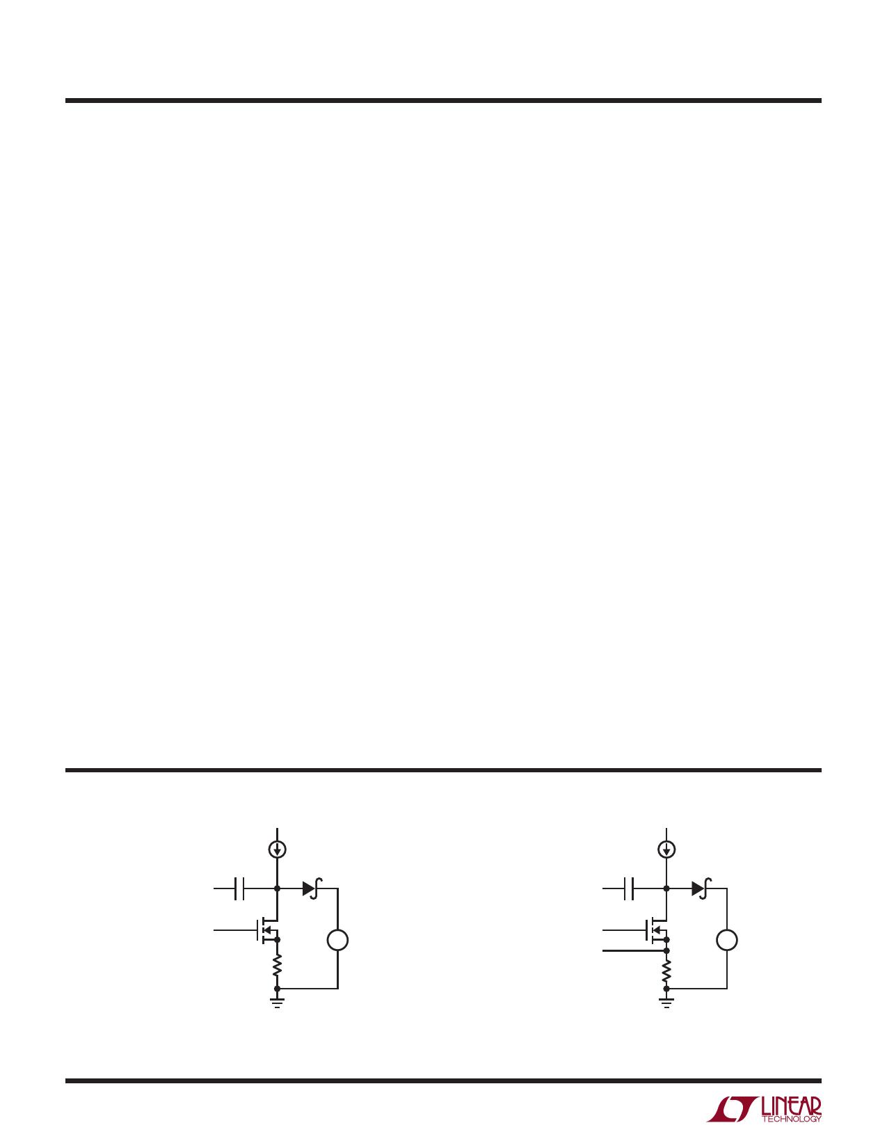
TEST CIRCUITS
5pF
CAP A/CAP B
20mA
IN5819
GATE A/GATE B
ZVN3306A –+ 10
2
1683 F01a
Figure 1a. Typical Test Circuitry
8
5pF
CAP A/CAP B
0.9A
IN5819
GATE A/GATE B
CS
Si4450DY –+ 10
0.1
1683 F01b
Figure 1b. Test Circuit for Slew
1683fd
Share Link: 