AD743JR-16-REEL7 Просмотр технического описания (PDF) - Analog Devices
Номер в каталоге
Компоненты Описание
Список матч
AD743JR-16-REEL7 Datasheet PDF : 12 Pages
| |||
AD743
HOW CHIP PACKAGE TYPE AND POWER DISSIPATION
AFFECT INPUT BIAS CURRENT
As with all JFET input amplifiers, the input bias current of
the AD743 is a direct function of device junction temperature,
IB approximately doubling every 10°C. Figure 8 shows the rela-
tionship between the bias current and the junction temperature
for the AD743. This graph shows that lowering the junction
temperature will dramatically improve IB.
10–6
300
TA = +25 C
200
JA = 115 C/W
100
JA = 165 C/W
JA = 0 C/W
10–7
10–8
10–9
TA = 25؇C
VS = ±15V
10–10
10–11
10–12
–60 –40 –20 0
20 40 60 80 100 120 140
JUNCTION TEMPERATURE (؇C)
Figure 8. Input Bias Current vs. Junction Temperature
The dc thermal properties of an IC can be closely approximated
by using the simple model of Figure 9, where current represents
power dissipation, voltage represents temperature, and resistors
represent thermal resistance ( in °C/W).
TJ JC
CA
PIN
JA
TA
PIN = DEVICE DISSIPATION
TA = AMBIENT TEMPERATURE
TJ = JUNCTION TEMPERATURE
JC = THERMAL RESISTANCE—JUNCTION TO CASE
CA = THERMAL RESISTANCE—CASE TO AMBIENT
Figure 9. Device Thermal Model
From this model, TJ = TA + JA PIN. Therefore, IB can be deter-
mined in a particular application by using Figure 8 together with
the published data for JA and power dissipation. The user can
modify JA by using of an appropriate clip-on heat sink, such as
the Aavid No. 5801. JA is also a variable when using the AD743
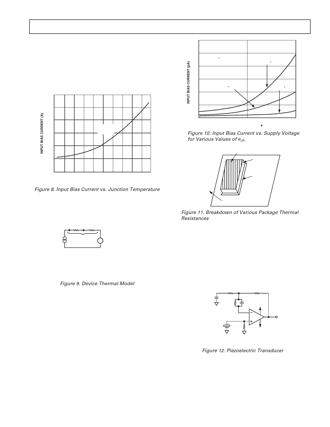
in chip form. Figure 10 shows the bias current versus the supply
voltage with JA as the third variable. This graph can be used to
predict bias current after JA has been computed. Again, bias cur-
rent will double for every 10°C. The designer using the AD743
in chip form (Figure 11) must also be concerned with both
JC and CA, since JC can be affected by the type of die mount
technology used.
Typically, JC will be in the 3°C/W to 5°C/W range; therefore,
for normal packages, this small power dissipation level may be
ignored. But, with a large hybrid substrate, JC will dominate
proportionately more of the total JA.
0
5
10
15
SUPPLY VOLTAGE ( V)
Figure 10. Input Bias Current vs. Supply Voltage
for Various Values of JA
TJ
A
(J TO
DIE MOUNT)
B
(DIE MOUNT
TO CASE)
TA
CASE
A + B = JC
Figure 11. Breakdown of Various Package Thermal
Resistances
REDUCED POWER SUPPLY OPERATION FOR LOWER IB
Reduced power supply operation lowers IB in two ways: first, by
lowering both the total power dissipation and second, by reduc-
ing the basic gate-to-junction leakage (Figure 10). Figure 12
shows a 40 dB gain piezoelectric transducer amplifier, which
operates without an ac-coupling capacitor over the –40°C to
+85°C temperature range. If the optional coupling capacitor is
used, this circuit will operate over the entire –55°C to +125°C
military temperature range.
100⍀
C1*
108⍀**
10k⍀
CT** +5V
TRANSDUCER
CT
108⍀
AD743
–5V
*OPTIONAL DC BLOCKING CAPACITOR
**OPTIONAL, SEE TEXT
Figure 12. Piezoelectric Transducer
REV. E
–9–
Share Link: 