AD7890(RevA) Просмотр технического описания (PDF) - Analog Devices
Номер в каталоге
Компоненты Описание
Список матч
AD7890 Datasheet PDF : 20 Pages
| |||
AD7890
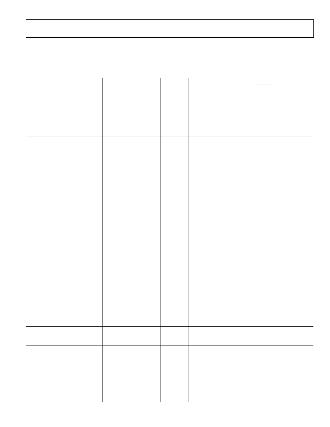
TIMING CHARACTERISTICS1, 2 (VDD = +5 V ؎ 5%, AGND = DGND = 0 V, REF IN = +2.5 V, fCLK IN = 2.5 MHz external, MUX OUT
connected to SHA IN.)
Parameter
Limit at TMIN, TMAX
(A, B, S Versions)
Units
Conditions/Comments
fCLKIN3
tCLK IN LO
tCLK IN HI
tr4
tf4
tCONVERT
tCST
Self-Clocking Mode
t1
t25
t3
t4
t55
t6
t76
t8
t9
t10
t11
t12
External-Clocking Mode
t13
t145
t15
t16
t175
t18
t196
t19A6
t20
t21
t22
t23
100
2.5
0.3 × tCLK IN
0 3 × tCLK IN
25
25
5.9
100
tCLK IN HI + 50
25
tCLK IN HI
tCLK IN LO
20
40
50
0
tCLK IN + 50
0
20
10
20
20
40
50
50
35
20
50
90
20
10
15
40
kHz min
MHz max
ns min
ns min
ns max
ns max
µs max
ns min
ns max
ns max
ns nom
ns nom
ns max
ns max
ns max
ns min
ns max
ns min
ns min
ns min
ns min
ns min
ns max
ns min
ns min
ns max
ns min
ns max
ns max
ns min
ns min
ns min
ns min
Master Clock Frequency. For Specified Performance
Master Clock Input Low Time
Master Clock Input High Time
Digital Output Rise Time. Typically 10 ns
Digital Output Fall Time. Typically 10 ns
Conversion Time
CONVST Pulse Width
RFS Low to SCLK Falling Edge
RFS Low to Data Valid Delay
SCLK High Pulse Width
SCLK Low Pulse Width
SCLK Rising Edge to Data Valid Delay
SCLK Rising Edge to RFS Delay
Bus Relinquish Time after Rising Edge of SCLK
TFS Low to SCLK Falling Edge
Data Valid to TFS Falling Edge Setup Time (A2 Address Bit)
Data Valid to SCLK Falling Edge Setup Time
Data Valid to SCLK Falling Edge Hold Time
TFS to SCLK Falling Edge Hold Time
RFS Low to SCLK Falling Edge Setup Time
RFS Low to Data Valid Delay
SCLK High Pulse Width
SCLK Low Pulse Width
SCLK Rising Edge to Data Valid Delay
RFS to SCLK Falling Edge Hold Time
Bus Relinquish Time after Rising Edge of RFS
Bus Relinquish Time after Rising Edge of SCLK
TFS Low to SCLK Falling Edge Setup Time
Data Valid to SCLK Falling Edge Setup Time
Data Valid to SCLK Falling Edge Hold Time
TFS to SCLK Falling Edge Hold Time
NOTES
1Sample tested at –25°C to ensure compliance. All input signals are specified with tr = tf = 5 ns (10% to 90% of 5 V) and timed from a voltage level of 1.6 V.
2See Figures 8 to 11.
3The AD7890 is production tested with fCLK IN at 2.5 MHz. It is guaranteed by characterization to operate at 100 kHz.
4Specified using 10% and 90% points on waveform of interest.
5These numbers are measured with the load circuit of Figure I and defined as the time required for the output to cross 0.8 V or 2.4 V.
6These numbers are derived from the measured time taken by the data output to change 0.5 V when loaded with the circuit of Figure 1. The measured number is then
extrapolated back to remove effects of charging or discharging the 50 pF capacitor. This means that the times quoted in the timing characteristics are the true bus re-
linquish times of the part and as such are independent of external bus loading capacitances.
1.6mA
TO OUTPUT
PIN
50pF
+2.1V
200µA
Figure 1. Load Circuit for Access Time and Bus Relinquish Time
–4–
REV. A
Share Link: 