MC10H116 Просмотр технического описания (PDF) - ON Semiconductor
Номер в каталоге
Компоненты Описание
Список матч
MC10H116 Datasheet PDF : 6 Pages
| |||
MC10H116
Triple Line Receiver
Description
The MC10H116 is a triple differential amplifier designed for use in
sensing differential signals over long lines and is a functional/pinout
duplication of the MC10116, with 100% improvement in propagation
delay and no increase in power supply current. For termination
information see AND8020.
Features
• Propagation Delay, 1.0 ns Typical
• Power Dissipation 85 mW Typ/Pkg (same as MECL 10K™)
• Improved Noise Margin 150 mV (Over Operating Voltage and
Temperature Range)
• Voltage Compensated
• MECL 10K Compatible
• Pb−Free Packages are Available*
4
2
5
3
9
6
10
7
12
14
13
15
11
VBB*
VCC1 = Pin 1
VCC2 = Pin 16
VEE = Pin 8
When input pin with
bubble goes positive
it’s respective output
pin with bubble goes
positive.
*VBB to be used to supply bias to the MC10H116 only and bypassed
(when used) with 0.01 mF to 0.1 mF capacitor to ground (0 V). VBB can
source < 1.0 mA.
The MC10H116 is designed to be used in sensing differential signals
over long lines. The bias supply (VBB) is made available to make the
device useful as a Schmitt trigger, or in other applications where a
stable reference voltage is necessary.
Active current sources provide these receivers with excellent
common−mode noise rejection. If any amplifier in a package is not
used, one input of that amplifier must be connected to VBB to prevent
unbalancing the current−source bias network.
The MC10H116 does not have internal−input pull− down resistors.
This provides high impedance to the amplifier input and facilitates
differential connections.
Applications:
• Low Level Receiver • Voltage Level
• Schmitt Trigger
Interface
Figure 1. Logic Diagram
VCC1
1
16
VCC2
AOUT
2
15
COUT
AOUT
3
14
COUT
AIN
4
13
CIN
AIN
5
12
CIN
BOUT
6
11
VBB
BOUT
7
10
BIN
VEE
8
9
BIN
Pin assignment is for Dual−in−Line Package.
For PLCC pin assignment, see TND309, the Pin Conversion Tables,
page 9.
Figure 2. Dip Pin Assignment
*For additional information on our Pb−Free strategy and soldering details, please
download the ON Semiconductor Soldering and Mounting Techniques
Reference Manual, SOLDERRM/D.
http://onsemi.com
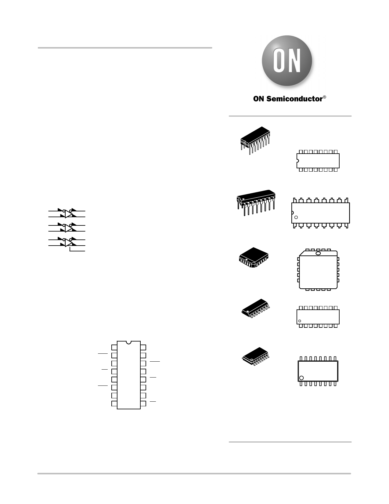
MARKING DIAGRAMS*
16
1
CDIP−16
L SUFFIX
CASE 620A
16
MC10H116L
AWLYYWW
1
16
1
PDIP−16
P SUFFIX
CASE 648
16
MC10H116P
AWLYYWWG
1
1 20
20 1
PLCC−20
FN SUFFIX
CASE 775
10H116G
AWLYYWW
16
1
SO−16
D SUFFIX
CASE 751B
16
10H116G
AWLYWW
1
16
1
SOEIAJ−16
M, MEL SUFFIX
CASE 966
16
10H116
ALYWG
1
A
= Assembly Location
WL = Wafer Lot
YY
= Year
WW = Work Week
*For additional marking information, refer to
Application Note AND8002/D.
ORDERING INFORMATION
See detailed ordering and shipping information in the package
dimensions section on page 3 of this data sheet.
© Semiconductor Components Industries, LLC, 2006
1
February, 2006 − Rev. 10
Publication Order Number:
MC10H116/D
Share Link: 