L294(1991) Просмотр технического описания (PDF) - STMicroelectronics
Номер в каталоге
Компоненты Описание
Список матч
L294 Datasheet PDF : 8 Pages
| |||
L294
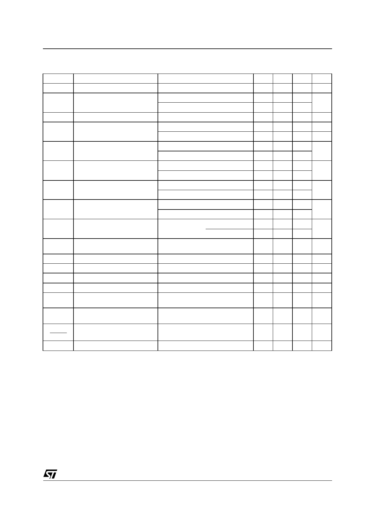
ELECTRICAL CHARACTERISTICS (refer to the test circuit, Vs = 40 V, Vss = 5V, Tamb = 25 °C, unless
otherwise specified)
Symbol
Vs
Id
Parameter
Power Supply Voltage (pin 1)
Quiescent Drain Current (pin 1)
Vss
Logic Suply Voltage (pin 4)
Iss
Quiescent Logic Supply
Current
Vi
Input Voltage (pin 7)
Ii
Input Current (pin 7)
VENABLE Enable Input Voltage (pin 9)
IENABLE Enable Input Current (pin 9)
Iload/ Vi Trasconductance
Vsat H
Source Output Saturation
Voltage
Vsat L Sink Output Saturation Voltage
Vsat H + VsatL Total Saturation Voltage
Ileakage Output Leakage Current
K
On Time Limiter Constant (°)
VDIAG
Diagnostic Output Voltage
(pin 5)
Test conditions
Operative Condition
VENABLE = H
Vi ≥ 0.6V; VENABLE = L
VDIAG = L
DIAG Output at High Impedance
Operating Output
Non-operative Output
Vi ≥ 0.6V
Vi ≤ 0.45V
Low Level
High Level
VENABLE = L
VENABLE = H
RS = 0.2 Ω
Vi = 1V
Vi = 4V
Ip = 4A
Ip = 4A
Ip = 4A
Rs = 0.2Ω; Vi ≤ 0.45 V
VENABLE = L
IDIAG = 10 mA
Min. Typ. Max. Unit
12
46
V
20 30
mA
70
4.5
7
V
5
8 mA
10 100 µA
0.6
V
0.45
-1
µA
-3
-0.3
0.8
V
2.4
-100 µA
100
0.95 1 1.05
A/V
0.97 1
1.3
1.7
V
2
V
4.5
V
1
mA
120
0.4
V
IDIAG
Vpin 8
Vp in 10
VSENS
Diagnostic Leakage Current
(pin 5)
OP AMP and OTA CD Voltage
Gain (°°)
Sensing Voltage (pin 10) (°°°)
VDIAG = 40V
Vpin 10 = 100 to 800 mV
10 µA
5
0.9 V
(°) After a time interval tmax = KC2, the output stages are disabled.
(°°) See the block diagram.
(°°°) Allowed range of VSENS without intervention of the short circuit protection.
3/8
Share Link: 