W83194R-KX Просмотр технического описания (PDF) - Winbond
Номер в каталоге
Компоненты Описание
Список матч
W83194R-KX Datasheet PDF : 13 Pages
| |||
W83194R-KX
PRELIMINARY
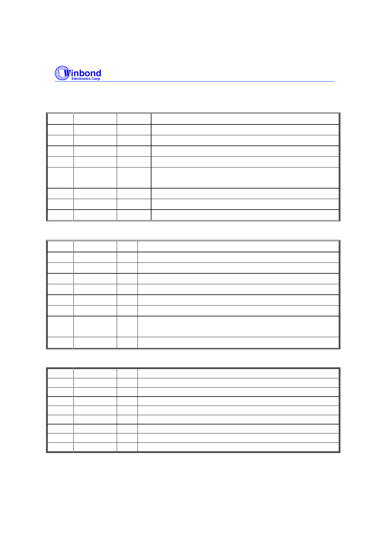
8.3.1 Register 0: Frequency Select Register (default = 0)
Bit @PowerUp
Pin
Description
7
0
6
0
5
0
4
0
-
Reserved
-
SSEL2 (for frequency table selection by software via I2C)
-
SSEL1 (for frequency table selection by software via I2C)
-
SSEL0 (for frequency table selection by software via I2C)
3
0
2
0
-
0 = Selection by hardware
1 = Selection by software I2C - Bit 6:4, Bit2
-
SSEL3 (for frequency table selection by software via I2C)
1
0
-
Reserved
0
0
-
Reserved
8.3.2 Register 1 : CPU Clock Register (1 = enable, 0 = Stopped)
Bit @PowerUp Pin
Description
7
0
- Reserved
6
0
- Reserved
5
0
- Reserved
4
0
- Reserved
3
1
40 SDRAM12 (Active / Inactive)
2
0
- Reserved
1
1
43 CPUT0
44 CPUC0 (Active / Inactive)
1
46 CPUT_CS (Active / Inactive)
8.3.3 Register 2: PCI Clock Register (1 = enable, 0 = Stopped)
Bit @PowerUp Pin
Description
7
1
- Reserved
6
1
7 PCICLK0 (Active / Inactive)
5
1
- Reserved
4
1
13 PCICLK5 (Active / Inactive)
3
1
12 PCICLK4 (Active / Inactive)
2
1
11 PCICLK3 (Active / Inactive)
1
1
10 PCICLK2(Active / Inactive)
0
1
8 PCICLK1 (Active / Inactive)
Publication Release Date: Nov. 1999
-9-
Revision 0.35
Share Link: 