CS5451-BS Просмотр технического описания (PDF) - Cirrus Logic
Номер в каталоге
Компоненты Описание
Список матч
CS5451-BS Datasheet PDF : 14 Pages
| |||
CS5451
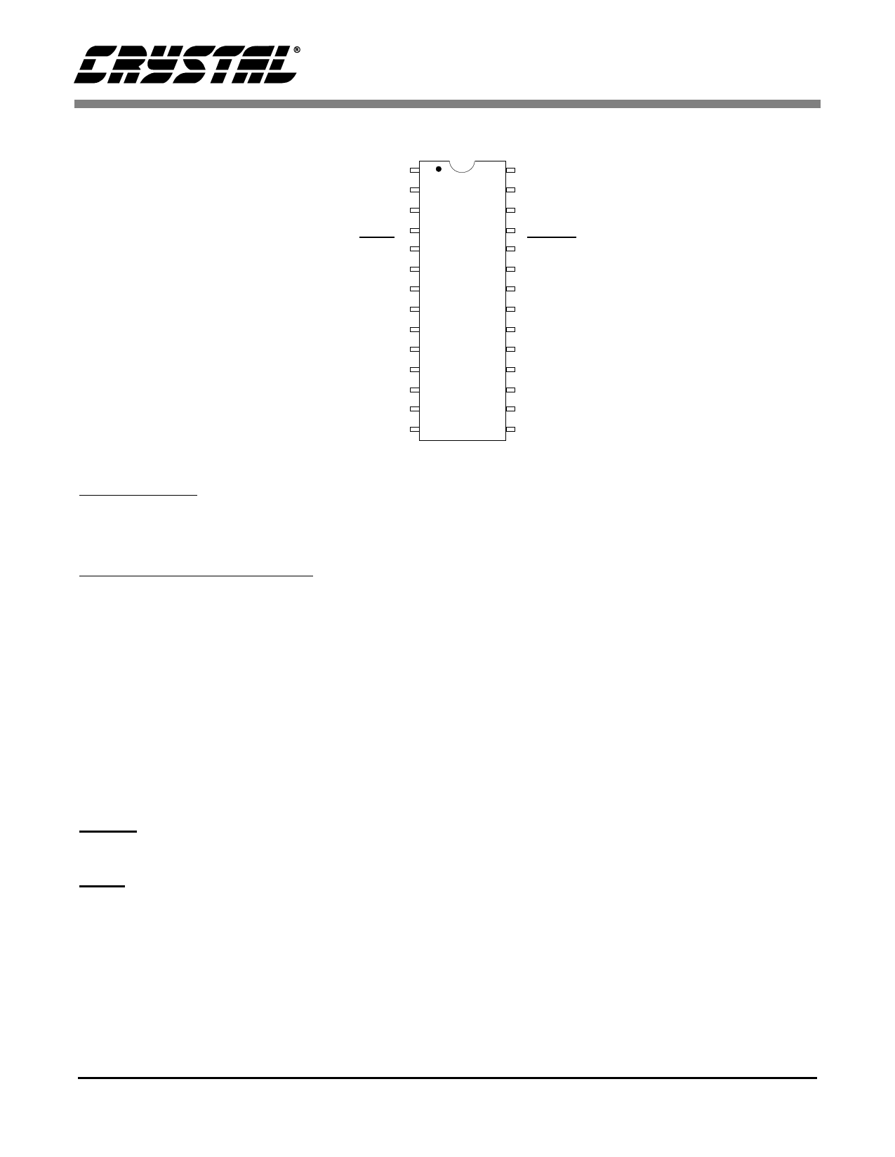
3. PIN DESCRIPTION
Serial Clock Output
SCLK 1
Serial Data Output
SDO 2
Frame Sync
FSO 3
Serial Port Enable
SE 4
Current Input Gain
GAIN 5
Analog Ground
AGND 6
Reference Input VREFIN 7
Reference Output VREFOUT 8
Positive Analog Supply
VA+ 9
Negative Analog Supply
VA- 10
Differential Voltage Input 3
VIN3+ 11
Differential Voltage Input 3
VIN3- 12
Differential Current Input 3
IIN3+ 13
Differential Current Input 3
IIN3- 14
28 VD+
27 DGND
26 CPD
25 XIN
24 RESET
23 OWRS
22 VIN1+
21 VIN1-
20 IIN1+
19 IIN1-
18 VIN2+
17 VIN2-
16 IIN2+
15 IIN2-
Digital Supply
Digital Ground
Charge Pump Drive
Master Clock
Reset
Output Word Rate Select
Differential Voltage Input 1
Differential Voltage Input 1
Differential Current Input 1
Differential Current Input 1
Differential Voltage Input 2
Differential Voltage Input 2
Differential Current Input 2
Differential Current Input 2
Clock Generator
XIN - Master Clock Input
Control Pins and Serial Data I/O
SE - Serial Port Enable
When SE is low, the output pins of the serial port are 3-stated.
SDO - Serial Port Output
Data will be at a rate determined by SCLK.
FSO - Frame Signal Output
Framing signal output for data transfer from SDO pin.
SCLK - Serial Clock Output
A clock signal on this pin determines the output rate of data for SDO pin. Rate of SCLK is determined
by XIN frequency and state of OWRS input pin.
RESET - Reset
When reset is taken low, all internal registers are set to their default states.
GAIN - Input Gain Control
Sets input gain for current channels. A logic high sets internal gain to 1, a logic low level sets the gain
to 20. If no connection is made to this pin, it will default to logic low level (through internal 200K
resistor to DGND).
OWRS - Output Word Rate Select
When OWRS is set to logic low, the output word rate (OWR) at SDO pin is XIN/2048 (Hz). When set to
logic high, the OWR at SDO pin is XIN/1024 (Hz). If no connection is made to this pin, then OWRS will
default to logic low level (through internal 200K resistor to DGND).
DS458PP4
11
Share Link: 