HA-5147-2 Просмотр технического описания (PDF) - Intersil
Номер в каталоге
Компоненты Описание
Список матч
HA-5147-2 Datasheet PDF : 11 Pages
| |||
HA-5147
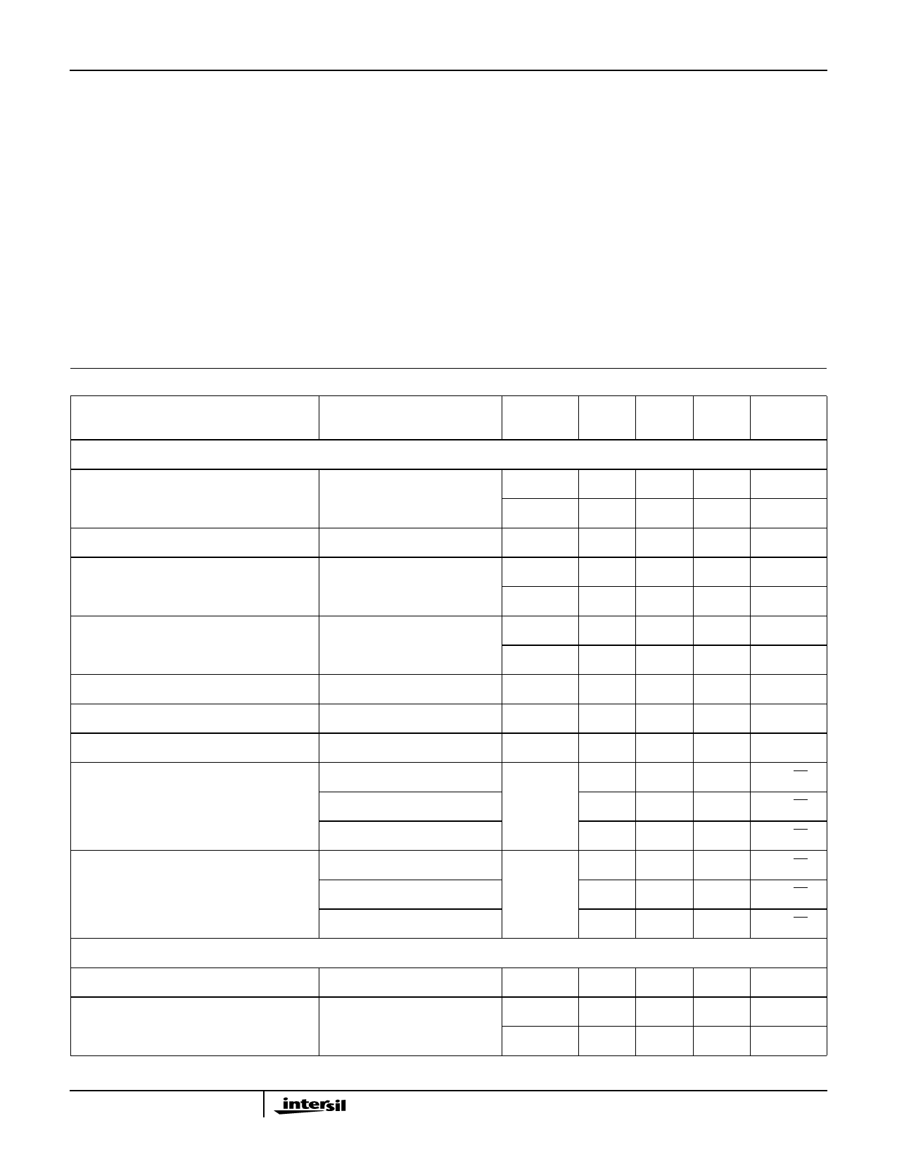
Absolute Maximum Ratings TA = 25oC
Voltage Between V+ and V- Terminals. . . . . . . . . . . . . . . . . . . . 44V
Differential Input Voltage (Note 1) . . . . . . . . . . . . . . . . . . . . . . . 0.7V
Output Current . . . . . . . . . . . . . . . . . . . Full Short Circuit Protection
Operating Conditions
Temperature Range
HA-5147-2 . . . . . . . . . . . . . . . . . . . . . . . . . . . . . . -55oC to 125oC
HA-5147-5 . . . . . . . . . . . . . . . . . . . . . . . . . . . . . . . . 0oC to 75oC
HA-5147-9 . . . . . . . . . . . . . . . . . . . . . . . . . . . . . . . -40oC to 85oC
Thermal Information
Thermal Resistance (Typical, Note 2)
θJA (oC/W) θJC (oC/W)
CERDIP Package. . . . . . . . . . . . . . . . . 135
50
SOIC Package . . . . . . . . . . . . . . . . . . . 158
N/A
Maximum Junction Temperature (Hermetic Package) . . . . . . . .175oC
Maximum Junction Temperature (Plastic Package) . . . . . . . . . .150oC
Maximum Storage Temperature Range . . . . . . . . . . -65oC to 150oC
Maximum Lead Temperature (Soldering 10s) . . . . . . . . . . . . 300oC
(SOIC - Lead Tips Only)
CAUTION: Stresses above those listed in “Absolute Maximum Ratings” may cause permanent damage to the device. This is a stress only rating and operation of the
device at these or any other conditions above those indicated in the operational sections of this specification is not implied.
NOTES:
1. For differential input voltages greater than 0.7V, the input current must be limited to 25mA to protect the back-to-back input diodes.
2. θJA is measured with the component mounted on an evaluation PC board in free air.
Electrical Specifications VSUPPLY = ±15V, CL ≤ 50pF, RS ≤ 100Ω
PARAMETER
TEST CONDITIONS
TEMP.
(oC)
MIN
TYP
MAX
UNITS
INPUT CHARACTERISTICS
Offset Voltage
25
-
30
100
µV
Average Offset Voltage Drift
Full
-
70
300
µV
Full
-
0.4
1.8
µV/oC
Bias Current
25
-
15
80
nA
Full
-
35
150
nA
Offset Current
25
-
12
75
nA
Full
-
30
135
nA
Common Mode Range
Full
±10.3 ±11.5
-
V
Differential Input Resistance (Note 3)
25
0.8
4
-
MΩ
Input Noise Voltage (Note 4)
Input Noise Voltage Density (Note 5)
0.1Hz to 10Hz
f = 10Hz
25
-
0.09
0.25
µVP-P
25
-
3.8
8.0
nV/√Hz
f = 100Hz
-
3.3
4.5
nV/√Hz
f = 1000Hz
-
3.2
3.8
nV/√Hz
Input Noise Current Density (Note 5)
f = 10Hz
25
-
1.7
-
pA/√Hz
f = 100Hz
-
1.0
-
pA/√Hz
f = 1000Hz
-
0.4
0.6
pA/√Hz
TRANSFER CHARACTERISTICS
Minimum Stable Gain
25
10
-
-
V/V
Large Signal Voltage Gain
VOUT = ±10V, RL = 2kΩ
25
700
1500
-
Full
300
800
-
V/mV
V/mV
2
Share Link: 