AD642KH Просмотр технического описания (PDF) - Analog Devices
Номер в каталоге
Компоненты Описание
Список матч
AD642KH Datasheet PDF : 6 Pages
| |||
AD642
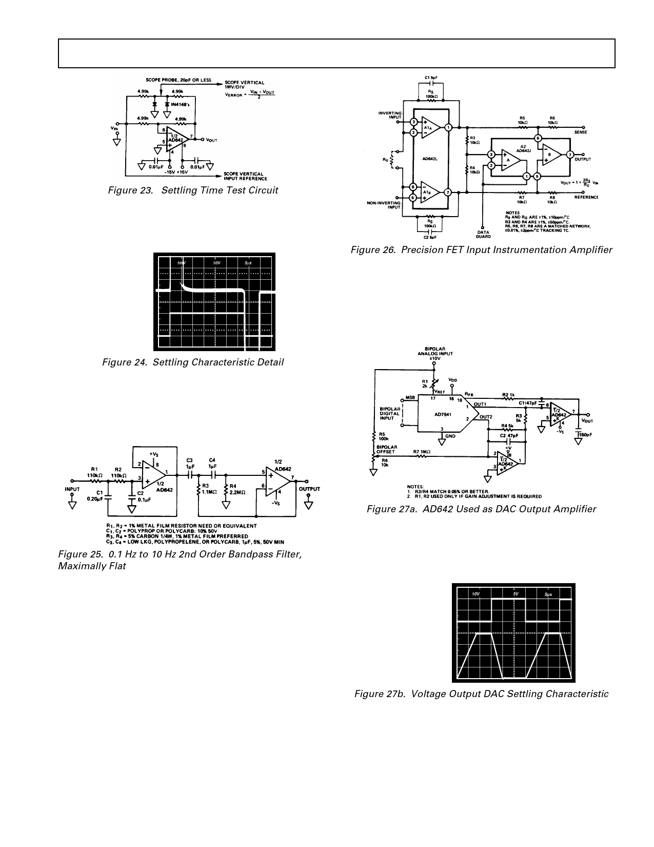
Figure 23. Settling Time Test Circuit
Fast settling time (8 µs to 0.01% for 20 V p-p step), low power
and low offset voltage make the AD642 an excellent choice for
use as an output amplifier for current output D/A converters
such as the AD7541.
1mV
10V
5µs
VERROR 1mV/DIV
INPUT 10V/DIV
Figure 24. Settling Characteristic Detail
The upper trace of the oscilloscope photograph of Figure 24
shows the settling characteristic of the AD642. The lower trace
represents the input to Figure 23. The AD642 has been
designed for fast settling to 0.01%, however, feedback compo-
nents, circuit layout and circuit design must be carefully
considered to obtain optimum settling time.
Figure 26. Precision FET Input Instrumentation Amplifier
The output impedance of a CMOS DAC varies with the digital
word thus changing the noise of the amplifier circuit. This effect
will cause a nonlinearity whose magnitude is dependent on the
offset voltage of the amplifier. The AD642K with trimmed
offset will minimize the effect. The Schottky protection diodes
recommended for use with many older CMOS DACs are not
required when using the AD642.
Figure 25. 0.1 Hz to 10 Hz 2nd Order Bandpass Filter,
Maximally Flat
The low frequency (1/f) noise has a power spectrum that is
inversely proportional to frequency. Typically this noise is not
important above 10 Hz, but it can be important for low fre-
quency-high gain applications.
The low noise characteristic of the AD642 make it ideal for 1/f
noise testing circuits. The circuit of Figure 25 is a 0.1 Hz to
10 Hz bandpass filter with second order filter characteristics.
The circuit illustrated in Figure 26 uses two AD642s to
construct an instrumentation amplifier with low input current
(35 pA max), high linearity and low offset voltage and offset
voltage drift. The AD644 may be substituted for increased
speed, but the higher open-loop gain of the AD642 maintains
better linearity over the gain range of 1 to 1000. Amplifier A1 is
an AD642L for low input offset voltage (250 µV max) and low
input offset voltage drift at high gains because matching and
tracking are very important for the balanced input stage.
Amplifier A2 serves two nonrelated functions, output amplifier
and active data-guard drive, and does not require close match-
ing between sections; thus it may be an AD642J.
Figure 27a. AD642 Used as DAC Output Amplifier
Figure 27a illustrates the AD7541 12-bit digital-to-analog
converter, connected for bipolar operation. Since the digital
input can accept bipolar numbers and VREF can accept a
bipolar analog input, the circuit can perform a 4-quadrant
multiplication.
10V
V REF IN , 2 0 V p -p , 3 3 k H z
10V/DIV VERT,
5µs/DIV HORIZ.
5V
5µs
V OUT
5V/DIV VERT,
5µs/DIV HORIZ.
SETTLING TIM E: 10µs TO
0.01% ON 20V STEP
Figure 27b. Voltage Output DAC Settling Characteristic
The photo above shows the output of the circuit Figure 27a.
The upper trace represents the reference input, and the bottom
trace shows the output voltage for a digital input of all ones on
the DAC. The 47 pF capacitor across the feedback resistor
compensates for the DAC output capacitance, and the 150 pF
load capacitor serves to minimize output glitches.
Log amplifiers or log ratio amplifiers are useful in applica-
tions requiring compression of wide-range analog input data,
REV. 0
–5–
Share Link: 