PI5C162214 Просмотр технического описания (PDF) - Pericom Semiconductor
Номер в каталоге
Компоненты Описание
Список матч
PI5C162214 Datasheet PDF : 3 Pages
| |||
PI5C16214
PI5C162214 (25Ω)
1122334455667788990011223344556677889900112233445566778899001122112233445566778899001122334455667788990011223344556677889900112211223344556677889900112233445566778899001122334455667788990011221122334455667788990011223344556677889900112233445566778899001122112233445566778899001122
12-Bit, 3-To-1 Bus-Select Switch
Features
• Near-zero propagation delay
• 5Ω switches connect inputs to outputs
• Direct bus connection when switches are ON
• Ultra-low quiescent power (0.2µA typical)
– ideally suited for notebook applications
• Industrial operating temperature: –40°C to +85°C
• Packages available:
– 56-pin 240-mil wide plastic TSSOP (A)
– 56-pin 300-mil wide plastic SSOP (V)
Product Description
Pericom Semiconductors PI5C series of BusSwitch circuits
are produced in the Companys advanced 0.8 micron CMOS
technology, achieving industry leading speed.
The PI5C16214 and PI5C162214 are 3-to-1 bus-select switches
designed with a low ON resistance (5Ω) allowing inputs to be
connected directly to outputs. These devices operate as 12-bit bus
switches via the data select pins (S0-S2).
The PI5C162214 device has a built-in 25-ohm series resistor to
reduce noise resulting from reflections, thus eliminating the need
for an external terminating resistor.
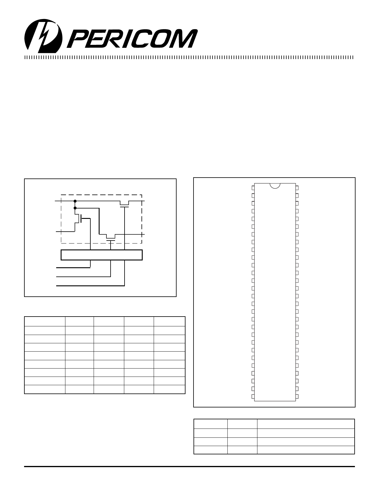
Logic Block Diagram
Product Pin Configuration
ONE OF TWELVE CHANNELS
1A1
1B1
1B3
1B2
FLOW CONTROL
S0
S1
S2
Truth Table(1)
Function
S2
S1
S0
A1
Disconnect
L
L
L
Z
A1 to B1
L
L
H
B1
A1 to B2
L
H
L
B2
Disconnect
L
H
H
Z
Disconnect
H
L
L
Z
A1 to B3
H
L
H
B3
A1 to B1
H
H
L
B1
A1 to B2
H
H
H
B2
Note:
1. H = High Voltage Level
L = Low Voltage Level
Z = High Impedance
S0
1A1
1B3
2A1
2B3
3A1
3B3
GND
4A1
4B3
5A1
5B3
6A1
6B3
7A1
7B3
VCC
8A1
GND
8B3
9A1
9B3
10A1
10B3
11A1
11B3
12A1
12B3
1
56
2
55
3
54
4
53
5
52
6
51
7
50
8
49
9
48
10
47
11
56-Pin
A, V
46
12
45
13
44
14
43
15
42
16
41
17
40
18
39
19
38
20
37
21
36
22
35
23
34
24
33
25
32
26
31
27
30
28
29
S1
S2
1B1
1B2
2B1
2B2
3B1
GND
3B2
4B1
4B2
5B1
5B2
6B1
6B2
7B1
7B2
8B1
GND
8B2
9B1
9B2
10B1
10B2
11B1
11B2
12B1
12B2
Product Pin Description
Pin Name I/O
Description
SO-S2
xAx
xBx
I
Select Inputs
I/O
Bus A
I/O
Bus B
1
PS7040A 04/23/99
Share Link: 