HI5735KCB(1998) Просмотр технического описания (PDF) - Intersil
Номер в каталоге
Компоненты Описание
Список матч
HI5735KCB Datasheet PDF : 12 Pages
| |||
HI5735
Noise Reduction
To reduce power supply noise, separate analog and digital
power supplies should be used with 0.1µF and 0.01µF
ceramic capacitors placed as close to the body of the
HI5735 as possible on the analog (AVEE) and digital (DVEE)
supplies. The analog and digital ground returns should be
connected together back at the device to ensure proper
operation on power up. The VCC power pin should also be
decoupled with a 0.1µF capacitor.
Reference
The internal reference of the HI5735 is a -1.23V (typical)
bandgap voltage reference with 50µV/oC of temperature drift
(typical). The internal reference is connected to the Control
Amplifier which in turn drives the segmented current cells.
Reference Out (REF OUT) is internally connected to the
Control Amplifier. The Control Amplifier Output (CTRL OUT)
should be used to drive the Control Amplifier Input (CTRL
IN) and a 0.1µF capacitor to analog VEE. This improves set-
tling time by providing an AC ground at the current source
base node. The Full Scale Output Current is controlled by
the REF OUT pin and the set resistor (RSET). The ratio is:
IOUT (Full Scale) = (VREF OUT/RSET) x 16.
The internal reference (REF OUT) can be overdriven with a
more precise external reference to provide better
performance over temperature. Figure 11 illustrates a typical
external reference configuration.
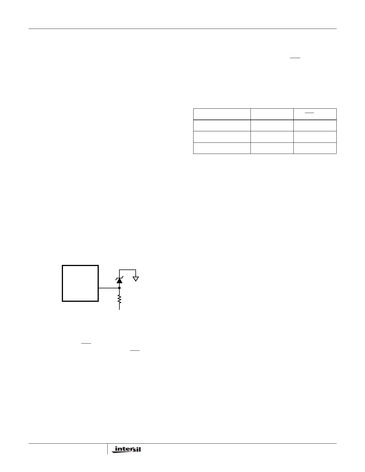
HI5735
(26) REF OUT
-1.25V
R
-5.2V
FIGURE 11. EXTERNAL REFERENCE CONFIGURATION
Outputs
The outputs IOUT and IOUT are complementary current
outputs. Current is steered to either IOUT or IOUT in proportion
to the digital input code. The sum of the two currents is always
equal to the full scale current minus one LSB. The current out-
put can be converted to a voltage by using a load resistor. Both
current outputs should have the same load resistor (64Ω typi-
cally). By using a 64Ω load on the output, a 50Ω effective output
resistance (ROUT) is achieved due to the 227Ω (±15%) parallel
resistance seen looking back into the output. This is the nomi-
nal value of the R2R ladder of the DAC. The 50Ω output is
needed for matching the output with a 50Ω line. The load resis-
tor should be chosen so that the effective output resistance
(ROUT) matches the line resistance. The output voltage is:
VOUT = IOUT x ROUT.
IOUT is defined in the reference section. IOUT is not trimmed
to 12 bits, so it is not recommended that it be used in
conjunction with IOUT in a differential-to-single-ended appli-
cation. The compliance range of the output is from -1.25V to
0V, with a 1VP-P voltage swing allowed within this range.
TABLE 2. INPUT CODING vs CURRENT OUTPUT
INPUT CODE (D11-D0)
1111 1111 1111
IOUT (mA)
-20.48
IOUT (mA)
0
1000 0000 0000
-10.24
-10.24
0000 0000 0000
0
-20.48
Settling Time
The settling time of the HI5735 is measured as the time it
takes for the output of the DAC to settle to within a 1/2 LSB
error band of its final value during a full scale (code 0000...
to 1111.... or 1111... to 0000...) transition. All claims made by
Intersil with respect to the settling time performance of the
HI5735 have been fully verified by the National Institute of
Standards and Technology (NIST) and are fully traceable.
Glitch
The output glitch of the HI5735 is measured by summing the
area under the switching transients after an update of the
DAC. Glitch is caused by the time skew between bits of the
incoming digital data. Typically, the switching time of digital
inputs are asymmetrical, meaning that the turn off time is
faster than the turn on time (TTL designs). Unequal delay
paths through the device can also cause one current source
to change before another. In order to minimize this, the Inter-
sil HI5735 employes an internal register, just prior to the cur-
rent sources, which is updated on the clock edge. Lastly, the
worst case glitch on traditional D/A converters usually occurs
at the major transition (i.e., code 2047 to 2048). However,
due to the split architecture of the HI5735, the glitch is
moved to the 255 to 256 transition (and every subsequent
256 code transitions thereafter). This split R/2R segmented
current source architecture, which decreases the amount of
current switching at any one time, makes the glitch practi-
cally constant over the entire output range. By making the
glitch a constant size over the entire output range, this effec-
tively integrates this error out of the end application.
In measuring the output glitch of the HI5735 the output is
terminated into a 64Ω load. The glitch is measured at any
one of the current cell carry (code 255 to 256 transition or
any multiple thereof) throughout the DACs output range.
The glitch energy is calculated by measuring the area under
the voltage-time curve. Figure 13 shows the area considered
as glitch when changing the DAC output. Units are typically
specified in picoVolt-seconds (pV-s).
HI5735
(21) IOUT
100MHz SCOPE
LOW PASS
FILTER
64Ω
50Ω
FIGURE 12. GLITCH TEST CIRCUIT
1628
Share Link: 