LTC1456C Просмотр технического описания (PDF) - Linear Technology
Номер в каталоге
Компоненты Описание
Список матч
LTC1456C Datasheet PDF : 8 Pages
| |||
LTC1456
PIN FUNCTIONS
CLK (Pin 1): The Serial Interface Clock. Internal Schmitt
trigger on this input allows direct optocoupler interface.
DIN (Pin 2): The Serial Interface Data. Data on the DIN pin
is latched into the shift register on the rising edge of the
serial clock.
CS/LD (Pin 3): The Serial Interface Enable and Load
Control. When CS/LD is low the CLK signal is enabled, so
the data can be clocked in. When CS/LD is pulled high,
data is loaded from the shift register into the DAC
register, updating the DAC output. When CS/LD is high
the CLK is disabled internally.
DOUT (Pin 4): The Output of the Shift Register Which
Becomes Valid on the Rising Edge of the Serial Clock.
GND (Pin 5): Ground.
CLR (Pin 6): The Clear Input. When pulled low, this pin
asynchronously clears the internal shift and DAC registers
to zero scale. Should be tied high for normal operation.
VOUT (Pin 7): The Buffered DAC Output.
VCC (Pin 8): The Positive Supply Input. 4.5V ≤ VCC ≤ 5.5V.
Requires a bypass capacitor to ground.
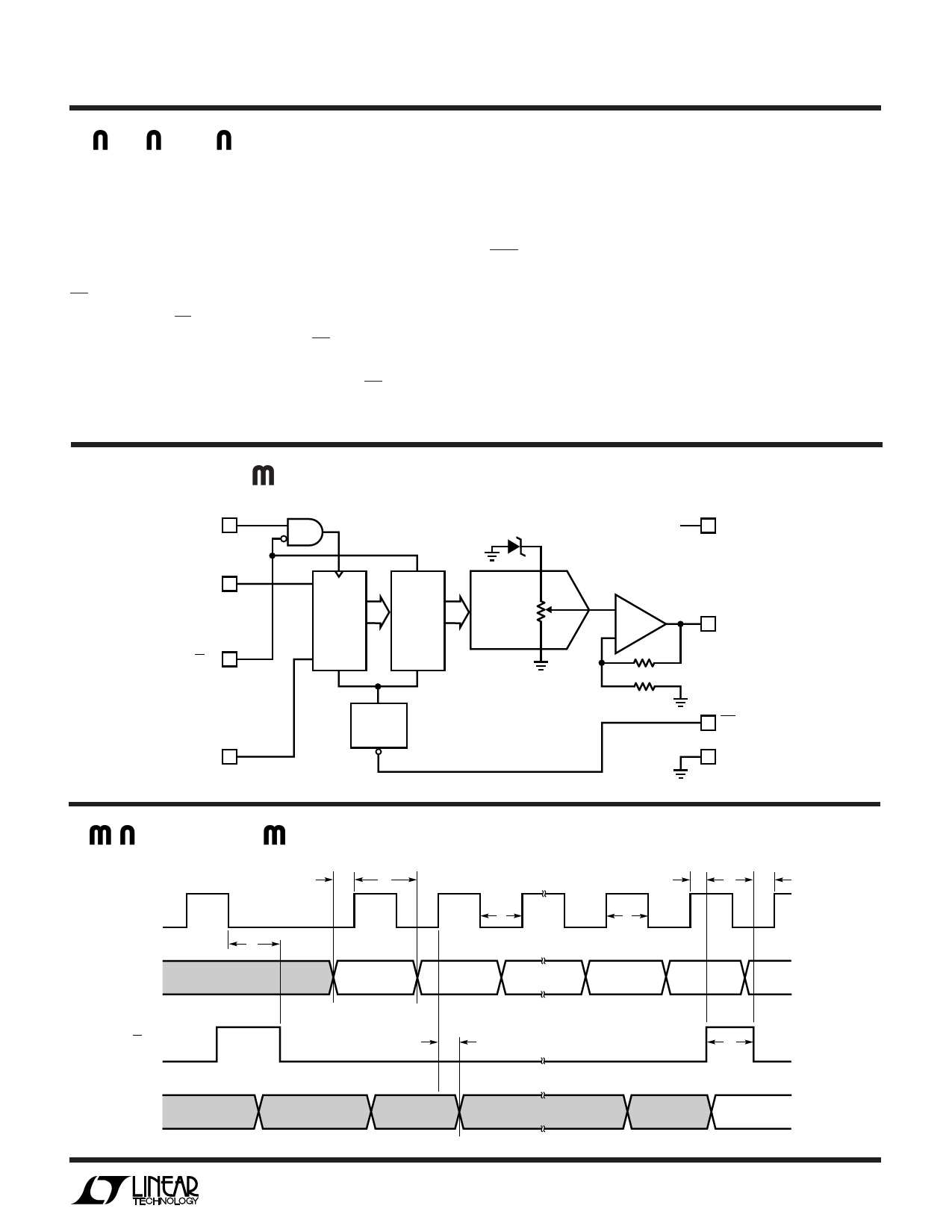
BLOCK DIAGRA
CLK 1
2.048V
8 VCC
DIN 2
CS/LD 3
12-BIT
SHIFT
REGISTER
LD
DAC
REGISTER
12-BIT
DAC
+
7 VOUT
–
DOUT 4
WU
W
TI I G DIAGRA
CLK
t9
DIN
B0
PREVIOUS WORD
CS/LD
POWER-ON
RESET
t1
t2
B11
MSB
t4
B10
t8
6 CLR
5 GND
1146 BD
t6
t7
t3
B1
B0
LSB
t5
DOUT
B11
PREVIOUS WORD
B10
B11
B1
B0
CURRENT WORD
1456 TD
5
Share Link: 