AD678KD Просмотр технического описания (PDF) - Analog Devices
Номер в каталоге
Компоненты Описание
Список матч
AD678KD Datasheet PDF : 14 Pages
| |||
AD678
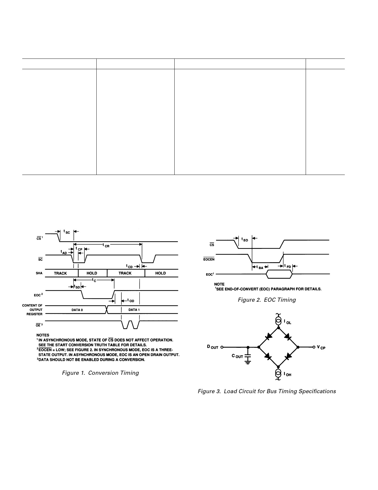
TIMING SPECIFICATIONS (All grades, TMIN to TMAX, VCC = +12 V ؎ 5%, VEE = –12 V ؎ 5%, VDD = +5 V ؎ 10% unless
otherwise noted)
Parameter
Symbol
Min
Max
SC Delay
tSC
Conversion Time
tC
Conversion Ratel
tCR
Convert Pulsewidth
tCP
Aperture Delay
tAD
Status Delay
tSD
Access Time2, 3
tBA
Float Delay5
tFD
Output Delay
tOD
Format Setup
tFS
OE Delay
tOE
Read Pulsewidth
tRP
Conversion Delay
tCD
EOCEN Delay
tEO
50
3.0
4.4
5
97
5
20
0
400
10
100
10
574
10
80
0
47
0
97
150
0
NOTES
1Includes acquisition time.
2Measured from the falling edge of OE/EOCEN (0.8 V) to the time at which the data lines/EOC cross 2.0 V or 0.8 V. See Figure 3.
3COUT = 100 pF.
4COUT = 50 pF.
5Measured from the rising edge of OE/EOCEN (2.0 V) to the time at which the output voltage changes by 0.5 V. See Figure 3; C OUT = 10 pF.
Specifications subject to change without notice.
Units
ns
µs
µs
ns
ns
ns
ns
ns
ns
ns
ns
ns
ns
ns
ns
Figure 2. EOC Timing
Figure 1. Conversion Timing
Figure 3. Load Circuit for Bus Timing Specifications
–4–
REV. C
Share Link: 