SAKC505L Просмотр технического описания (PDF) - Infineon Technologies
Номер в каталоге
Компоненты Описание
Список матч
SAKC505L Datasheet PDF : 85 Pages
| |||
C505L
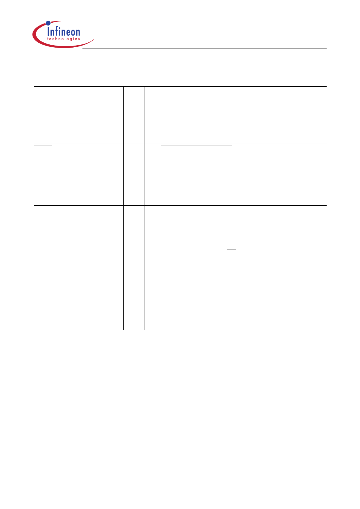
Table 1
Pin Definitions and Functions (cont’d)
Symbol
Pin Number I/O*) Function
RESET
43
PSEN
44
I
RESET
A high level on this pin for two machine cycles while the
oscillator is running resets the device. An internal diffused
resistor to VSS permits power-on reset using only an
external capacitor to VDD.
O The Program Store Enable
output is a control signal that enables the external program
memory to the bus during external fetch operations. It is
activated every three oscillator periods except during
external data memory accesses. Remains high during
internal program execution. This pin should not be driven
during reset operation.
ALE
45
O The Address Latch Enable
output is used for latching the low-byte of the address into
external memory during normal operation. It is activated
every three oscillator periods except during an external data
memory access. When instructions are executed from
internal program memory (EA = 1), the ALE generation can
be disabled by bit EALE in SFR SYSCON. This pin should
not be driven during reset operation.
EA
46
I
External Access Enable
This pin must be held at high level. Instructions are fetched
from the internal OTP memory when the PC is less than
8000H. Instructions are fetched from external program
memory, when the PC is greater than 7FFFH. This pin must
not be held at low level.
*) I = Input
O = Output
Data Sheet
8
06.99
Share Link: 