L4902A Просмотр технического описания (PDF) - STMicroelectronics
Номер в каталоге
Компоненты Описание
Список матч
L4902A Datasheet PDF : 9 Pages
| |||
L4902A
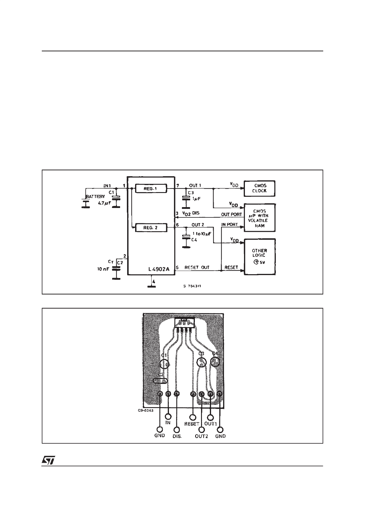
This output may thereforebe usedto supply circuits
continuously, such as volatile RAMs, allowing the
use of a back-up battery.
The V02 output can supply other non essential 5 V
circuits which may be powered down when the
system is inactive, or that must be powered down
to prevent uncorrect operation for supply voltages
below the minimum value.
The reset output can be usedas a ”POWERDOWN
INTERRUPT”, permitting RAM access only in cor-
rect power conditions, or as a ”BACK-UP ENABLE”
to transfer data into in a NV SHADOW MEMORY
Figure 2
when the supply is interrupted.
The disable function can be used for remote on/off
control of circuits connected to the V02 output.
APPLICATION SUGGESTIONS
Figure 2 illustrate how the L4902A’s disable input
may be used in a CMOS µComputer application.
TheV01 regulator(low consumption)supply perma-
nently a CMOS time of day clock and a CMOS
µcomputer chip with volatile memory. V02 output,
supplying non-essential circuits, is turned OFF un-
der control of a µP unit.
Figure 3 : P.C. Board Component Layout of Figure 2
5/9
Share Link: 