UT61L6416MC-12 Просмотр технического описания (PDF) - Utron Technology Inc
Номер в каталоге
Компоненты Описание
Список матч
UT61L6416MC-12 Datasheet PDF : 9 Pages
| |||
Rev. 1.0
UTRON
UT61L6416
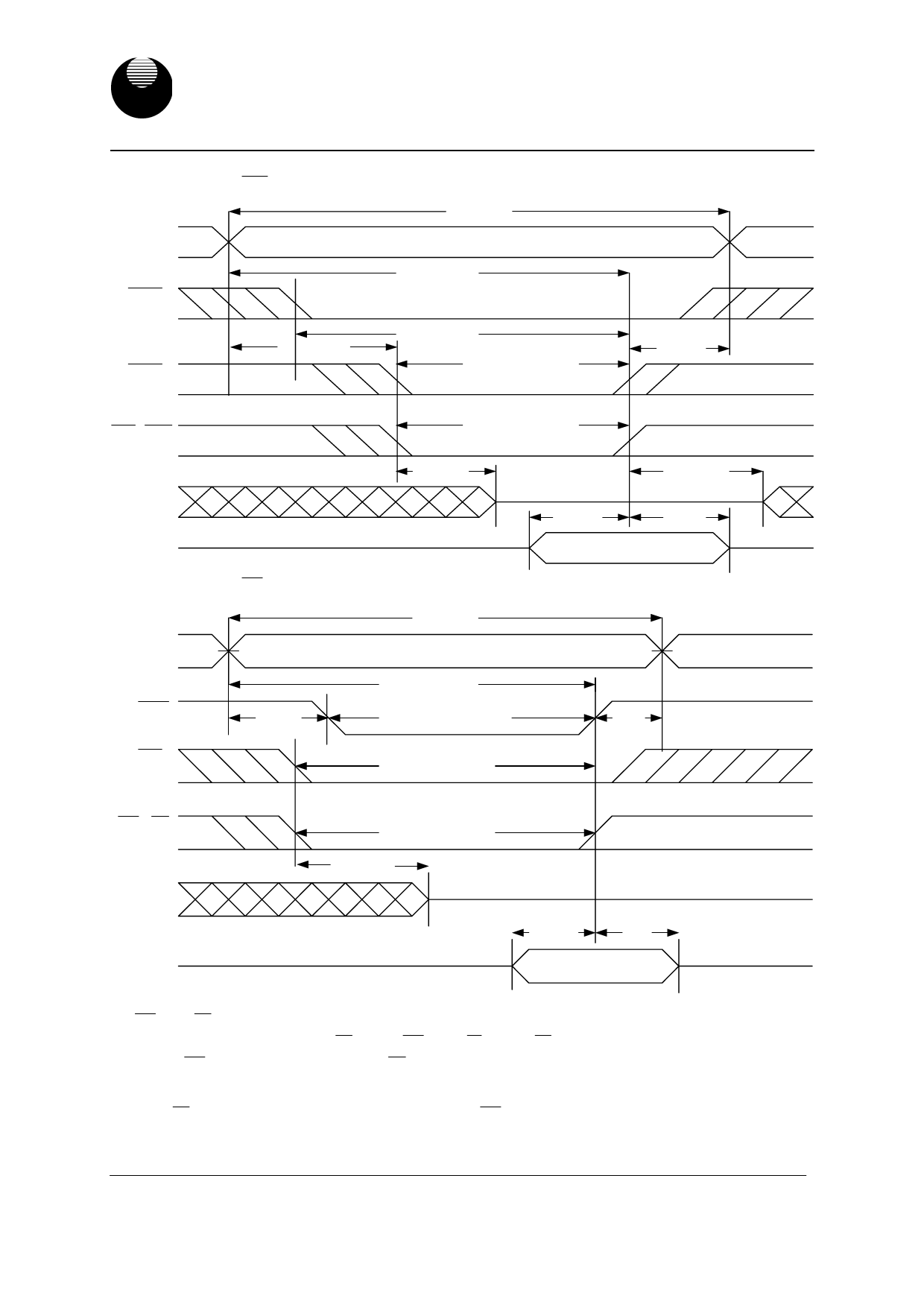
64K X 16 BIT HIGH SPEED CMOS SRAM
WRITE CYCLE 1 ( WE Controlled) (1,2,3,5,6)
t WC
Address
CE
WE
t AS
t AW
t CW
t WP
t WR
LB , UB
Dout
Din
t BW
t WHZ
(4)
High-Z
t DW
t OW
(4)
t DH
Data Valid
WRITE CYCLE 2 ( CE Controlled) (1,2,5)
t WC
Address
CE
t AS
t AW
t CW
t WR
WE
t WP
LB , UB
t BW
Dout
t WHZ
High-Z
t DW
t DH
Din
Data Valid
Notes :
1. WE and CE must be HIGH during all address transitions.
2. A write occurs during the overlap of CE = low , WE =low , LB and/or UB =low.
3. During a WE controlled with write cycle with OE LOW, tWP must be greater than tWHZ+tDW to allow the drivers to turn off and
data to be placed on the bus.
4. During this period, I/O pins are in the output state, and input signals must not be applied.
5. If the CE low transition occurs simultaneously with or after WE low transition, the outputs remain in a high impedance
state.
6. tOW and tWHZ are specified with CL = 5pF. Transition is measured ±500mV from steady state.
UTRON TECHNOLOGY INC.
1F, No. 11, R&D Rd. II, Science-Based Industrial Park, Hsinchu, Taiwan, R. O. C.
TEL: 886-3-5777882 FAX: 886-3-5777919
6
P80072
Share Link: 