IDT72805LB Просмотр технического описания (PDF) - Integrated Device Technology
Номер в каталоге
Компоненты Описание
Список матч
IDT72805LB
Integrated Device Technology

IDT72805LB Datasheet PDF : 26 Pages
| |||
CMOS DUAL SyncFIFO™
DUAL 256 x 18
IDT72805LB
DUAL 512 x 18
IDT72815LB
DUAL 1,024 x 18
IDT72825LB
DUAL 4,096 x 18
IDT72845LB
LEAD FINISH (SnPb) ARE IN EOL PROCESS - LAST TIME BUY EXPIRES JUNE 15, 2018
FEATURES:
• The IDT72805LB is equivalent to two IDT72205LB 256 x 18 FIFOs
• The IDT72815LB is equivalent to two IDT72215LB 512 x 18 FIFOs
• The IDT72825LB is equivalent to two IDT72225LB 1,024 x 18 FIFOs
• The IDT72845LB is equivalent to two IDT72245LB 4,096 x 18 FIFOs
• Offers optimal combination of large capacity (8K), high speed,
design flexibility, and small footprint
• Ideal for the following applications:
- Network switching
- Two level prioritization of parallel data
- Bidirectional data transfer
- Bus-matching between 18-bit and 36-bit data paths
- Width expansion to 36-bit per package
- Depth expansion to 8,192 words per package
• 10ns read/write cycle time, 6.5ns access time
• IDT Standard or First Word Fall Through timing
• Single or double register-buffered Empty and Full Flags
• Easily expandable in depth and width
• Asynchronous or coincident Read and Write clocks
• Asynchronous or synchronous programmable Almost-Empty
and Almost-Full flags with default settings
• Half-Full flag capability
• Output Enable puts output data bus in high-impedance state
• High-performance submicron CMOS technology
• Available in the 128-pin Thin Quad Flatpack (TQFP). Also
available for the IDT72805LB/72815LB/72825LB, in the 121-lead,
16 x 16 mm plastic Ball Grid Array (PBGA)
• Industrial temperature range (–40°C to +85°C) is available
• Green parts available, see ordering information
DESCRIPTION:
The IDT72805LB/72815LB/72825LB/72845LB are dual 18-bit-wide syn-
chronous (clocked) First-in, First-out (FIFO) memories. One dual IDT72805LB/
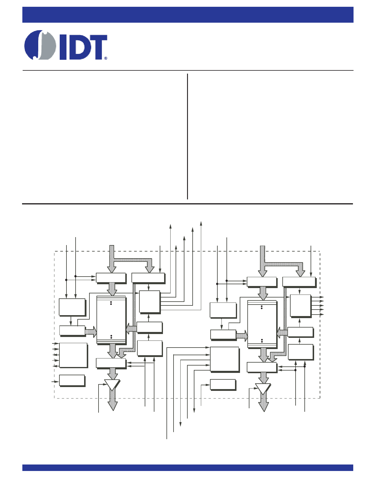
FUNCTIONAL BLOCK DIAGRAM
WCLKA
F
F A/IR
A EF
HF A/(WXOA)
P AEA
A/
ORA
WCLKB
WENA
DA0-DA17
L DA PAFA
WENB
DB0-DB17
L DB
INPUT
REGISTER
OFFSET
REGISTER
WRITE
CONTROL
LOGIC
WRITE
POINTER
FLA
WXIA
(HF A)/WXOA
RXIA
RXOA
EXPANSION
LOGIC
RESET
RSA
LOGIC
RAM
ARRAY
256 x 18
512 x 18
1,024 x 18
4,096 x 18
OUTPUT
REGISTER
FLAG
LOGIC
READ
POINTER
READ
CONTROL
LOGIC
INPUT
REGISTER
WRITE
CONTROL
LOGIC
WRITE
POINTER
RAM
ARRAY
256 x 18
512 x 18
1,024 x 18
4,096 x 18
EXPANSION
LOGIC
RESET
LOGIC
OUTPUT
REGISTER
OFFSET
REGISTER
FLAG
LOGIC
F F B/IRB
PAF B
EF B/ORB
P AEB
HF B/(WXOB)
READ
POINTER
READ
CONTROL
LOGIC
OEA QA0-QA17
RCLKA
RENA
RSB
RXOB
RXIB
(HF B)/WXOB
WXIB
FLB
OEB
QB0-QB17
IDT and the IDT logo are registered trademarks of Integrated Device Technology, Inc. The SyncFIFO is a trademark of Integrated Device Technology, Inc.
COMMERCIAL AND INDUSTRIAL TEMPERATURE RANGES
1
©2018 Integrated Device Technology, Inc. All rights reserved. Product specifications subject to change without notice.
RCLKB
RENB
3139 drw 01
MARCH 2018
DSC-3139/10
Share Link: